
Page 238 - Rashid, Power Electronics Handbook
P. 238
14 Inverters 227
In this chapter, single and three-phase inverters in their TABLE 14.1 Switch states for a half-bridge single-phase VSI
voltage and current source alternatives will be reviewed. The
dc link will be assumed to be a perfect dc, either voltage or State State # v o Components
Conducting
current source that could be ®xed as the dc link voltage in
standard ASDs, or variable as the dc link current in some S þ is on and S ÿ is off 1 v i =2 S þ if i o > 0
medium-voltage current source drives. Speci®cally, the topol- D þ if i o < 0
S ÿ is on and S þ is off 2 ÿv i =2 D ÿ if i o > 0
ogies, modulating techniques, and control aspects, oriented to
S ÿ if i o < 0
standard applications, are analyzed. In order to simplify the s þ and S ÿ are all off 3 ÿv i =2 D ÿ if i o > 0
analysis, the inverters are considered lossless topologies, which v i =2 D þ if i o < 0
are composed of ideal power valves. Nevertheless, some
practical nonideal conditions are also considered.
Figure 14.3 shows the ideal waveforms associated with the
half-bridge inverter shown in Fig. 14.2. The states for the
14.2 Single-Phase Voltage Source switches S and S are de®ned by the modulating technique,
þ
ÿ
Inverters which in this case is a carrier-based PWM.
Single-phase voltage source inverters (VSIs) can be found as 14.2.1.1 The Carrier-Based Pulsewidth Modulation
half-bridge and full-bridge topologies. Although the power (PWM) Technique
range they cover is the low one, they are widely used in power
As mentioned earlier, it is desired that the ac output voltage
supplies, single-phase UPSs, and currently to form elaborate
v ¼ v aN follow a given waveform (e.g., sinusoidal) on a
o
high-power static power topologies, such as for instance, the
continuous basis by properly switching the power valves.
multicell con®gurations that are reviewed in Section 14.7. The
The carrier-based PWM technique ful®ls such a requirement
main features of both approaches are reviewed and presented
as it de®nes the on and off states of the switches of one leg of a
in the following.
VSI by comparing a modulating signal v (desired ac output
c
voltage) and a triangular waveform v D (carrier signal). In
14.2.1 Half-Bridge VSI practice, when v > v the switch S þ is on and the switch
D
c
S is off; similarly, when v < v the switch S is off and the
D
c
ÿ
þ
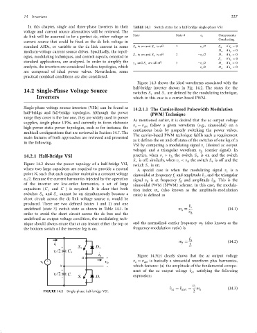
Figure 14.2 shows the power topology of a half-bridge VSI, switch S is on.
ÿ
where two large capacitors are required to provide a neutral A special case is when the modulating signal v is a
c
point N, such that each capacitor maintains a constant voltage sinusoidal at frequency f and amplitude ^ v , and the triangular
c
c
v =2. Because the current harmonics injected by the operation signal v D is at frequency f and amplitude ^ v . This is the
i
D
D
of the inverter are low-order harmonics, a set of large sinusoidal PWM (SPWM) scheme. In this case, the modula-
capacitors (C and C ) is required. It is clear that both
þ ÿ tion index m (also known as the amplitude-modulation
a
switches S and S cannot be on simultaneously because a
þ ÿ ratio) is de®ned as
short circuit across the dc link voltage source v would be
i
produced. There are two de®ned (states 1 and 2) and one
^ v c
unde®ned (state 3) switch state as shown in Table 14.1. In m ¼ ð14:1Þ
a ^ v
order to avoid the short circuit across the dc bus and the D
unde®ned ac output voltage condition, the modulating tech-
nique should always enure that at any instant either the top or and the normalized carrier frequency m (also known as the
f
the bottom switch of the inverter leg is on. frequency-modulation ratio) is
f D
m ¼ ð14:2Þ
f
f c
Figure 14.3(e) clearly shows that the ac output voltage
v ¼ v aN is basically a sinusoidal waveform plus harmonics,
o
which features: (a) the amplitude of the fundamental compo-
nent of the ac output voltage ^ v o1 satisfying the following
expression:
v i
^ v ¼ ^ v aN1 ¼ m a ð14:3Þ
o1
FIGURE 14.2 Single-phase half-bridge VSI. 2