Page 242 - Rashid, Power Electronics Handbook
P. 242

14  Inverters                                                                                       231

                 eliminate an odd N ÿ 1(N ÿ 1 ¼ 3; 5; 7; ...) number of  where V o1  is the fundamental rms ac output voltage, I is the
                                                                                                                  o
                 harmonics are given by                               rms load current, f is an arbitrary inductive load power factor,
                                                                      and I is the dc link current that can be further simpli®ed to
                                                                          i
                       N
                       P     k         2 ÿ p^ v =v i
                                             o1
                     ÿ   ðÿ1Þ cosðna Þ¼                                                     V
                                   k
                      k¼1                  4                                            I ¼  o1  I cosðfÞ          ð14:14Þ
                                                                                                o
                                                                                         i
                                                                                            V i
                       N
                       P     k         1
                     ÿ   ðÿ1Þ cosðna Þ¼     for n ¼ 3; 5; ... ; 2N ÿ 1
                                   k
                      k¼1              2                              14.2.2 Full-Bridge VSI
                                                              ð14:11Þ
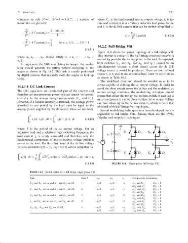
                                                                      Figure 14.8 shows the power topology of a full-bridge VSI.
                 where a ; a ; ... ; a N  should satisfy a < a <     < a <  This inverter is similar to the half-bridge inverter; however, a
                                                      2
                                                                N
                                                  1
                        1
                           2
                 p=2.                                                 second leg provides the neutral point to the load. As expected,
                                                                      both switches S  and S  (or S  and S ) cannot be on
                   To implement the SHE modulating technique, the modu-            1þ      1ÿ     2þ     2ÿ
                                                                      simultaneously because a short circuit across the dc link
                 lator should generate the gating pattern according to the
                                                                      voltage source v would be produced. There are four de®ned
                 angles as shown in Fig. 14.7. This task is usually performed      i
                                                                      (states 1, 2, 3, and 4) and one unde®ned (state 5) switch states
                 by digital systems that normally store the angles in look-up
                                                                      as shown in Table 14.2.
                 tables.
                                                                        The unde®ned condition should be avoided so as to be
                                                                      always capable of de®ning the ac output voltage. In order to
                 14.2.1.4 DC Link Current
                                                                      avoid the short circuit across the dc bus and the unde®ned ac
                 The split capacitors are considered part of the inverter and
                                                                      output voltage condition, the modulating technique should
                 therefore an instantaneous power balance cannot be consid-
                                                                      ensure that either the top or the bottom switch of each leg is
                 ered due to the storage energy components (C  and C ).
                                                          þ      ÿ    on at any instant. It can be observed that the ac output voltage
                 However, if a lossless inverter is assumed, the average power
                                                                      can take values up to the dc link value v , which is twice that
                                                                                                       i
                 absorbed in one period by the load must be equal to the
                                                                      obtained with half-bridge VSI topologies.
                 average power supplied by the dc source. Thus, we can write
                                                                        Several modulating techniques have been developed that are
                                                                      applicable to full-bridge VSIs. Among them are the PWM
                        ð                ð
                         T                T
                           v ðtÞ  i ðtÞ  dt ¼  v ðtÞ  i ðtÞ  dt  ð14:12Þ  (bipolar and unipolar) techniques.
                                            o
                                i
                            i
                                                 o
                         0                0
                 where T is the period of the ac output voltage. For an
                 inductive load and a relatively high switching frequency, the
                 load current i is nearly sinusoidal and therefore only the
                             o
                 fundamental component of the ac output voltage provides
                 power to the load. On the other hand, if the dc link voltage
                 remains constant v ðtÞ¼ V , Eq. (14.12) can be simpli®ed to
                                 i
                                       i
                 ð T         1  ð T  p      p 
                    i ðtÞ  dt ¼    2V sinðotÞ   2I sinðot ÿ fÞ  dt ¼ I
                    i                 o1          o                i
                  0          V i  0
                                                              ð14:13Þ           FIGURE 14.8  Single-phase full-bridge VSI.
                          TABLE 14.2  Switch states for a full-bridge single-phase VSI
                          State                            State #   v aN     v bN    v o    Components Conducting
                          S 1þ and S 2ÿ are on and S 1ÿ and S 2þ are off  1  v i =2  ÿv i =2  v i  S 1þ and S 2ÿ  if i o > 0
                                                                                                           if i o < 0
                                                                                             D 1þ and D 2ÿ
                          S 1ÿ and S 2þ are on and S 1þ and S 2ÿ are off  2  ÿv i =2  v i =2  ÿv i  D 1ÿ and D 2þ  if i o > 0
                                                                                                           if i o < 0
                                                                                             S 1ÿ and S 2þ
                          S 1þ and S 2þ are on and S 1ÿ and S 2ÿ are off  3  v i =2  v i =2  0  S 1þ and D 2þ  if i o > 0
                                                                                                           if i o < 0
                                                                                             D 1þ and S 2þ
                          s 1ÿ and S 2ÿ are on and S 1þ and S 2þ are off  4  ÿv i =2  ÿv i =2  0  D 1ÿ and S 2ÿ  if i o > 0
                                                                                                           if i o < 0
                                                                                             S 1ÿ and D 2ÿ
                          S 1ÿ , S 2ÿ , S 1þ , and S 2þ are all off  5  ÿv i =2  v i =2  ÿv i  D 1ÿ and D 2þ  if i o > 0
                                                                      v i =2  ÿv i =2  v i   D 1þ and D 2ÿ  if i o < 0
   237   238   239   240   241   242   243   244   245   246   247