
Page 246 - Rashid, Power Electronics Handbook
P. 246
14 Inverters 235
where V o1 is the fundamental rms ac output voltage, I is the
o
rms load current, and f is an arbitrary inductive load power
factor. Thus, the dc link current can be further simpli®ed to
V o1 V o1
i ðtÞ¼ I cosðfÞÿ I cosð2ot ÿ fÞ ð14:25Þ
i o o
V V
i i
The preceding expression reveals an important issue, that is,
the presence of a large second-order harmonic in the dc link
current (its amplitude is similar to the dc link current). This
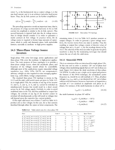
second harmonic is injected back into the dc voltage source, FIGURE 14.13 Three-phase VSI topology.
thus its design should consider it in order to guarantee a
nearly constant dc link voltage. In practical terms, the dc remaining states (1 to 6 in Table 14.3) produce nonzero ac
voltage source is required to feature large amounts of capaci- output voltages. In order to generate a given voltage wave-
tance, which is costly and demands space, both undesirable form, the inverter moves from one state to another. Thus the
features, especially in medium- to high-power supplies. resulting ac output line voltages consist of discrete values of
voltages that are v , 0, and ÿv for the topology shown in Fig.
i
i
14.3 Three-Phase Voltage Source 14.13. The selection of the states in order to generate the given
waveform is done by the modulating technique that should
Inverters
ensure the use of only the valid states.
Single-phase VSIs cover low-range power applications and
three-phase VSIs cover the medium- to high-power applica- 14.3.1 Sinusoidal PWM
tions. The main purpose of these topologies is to provide a
This is an extension of the one introduced for single-phase VSIs.
three-phase voltage source, where the amplitude, phase, and
In this case and in order to produce 120 out-of-phase load
frequency of the voltages should always be controllable.
voltages, three modulating signals that are 120 out of phase are
Although most of the applications require sinusoidal voltage
used. Figure 14.14 shows the ideal waveforms of three-phase
waveforms (e.g., ASDs, UPSs, FACTS, var compensators),
VSI SPWM. In order to use a single carrier signal and preserve
arbitrary voltages are also required in some emerging applica-
the features of the PWM technique, the normalized carrier
tions (e.g., active ®lters, voltage compensators).
frequency m should be an odd multiple of 3. Thus, all phase
f
The standard three-phase VSI topology is shown in Fig.
voltages (v , v , and v ) are identical but 120 out of phase
cN
bN
aN
14.13 and the eight valid switch states are given in Table 14.3.
without even harmonics; moreover, harmonics at frequencies a
As in single-phase VSIs, the switches of any leg of the inverter
multiple of 3 are identical in amplitude and phase in all
(S and S , S and S ,or S and S ) cannot be switched on phases. For instance, if the ninth harmonic in phase aN is
5
2
6
3
4
1
simultaneously because this would result in a short circuit
across the dc link voltage supply. Similarly, in order to avoid
v aN9 ðtÞ¼ ^ v sinð9otÞ ð14:26Þ
9
unde®ned states in the VSI, and thus unde®ned ac output line
voltages, the switches of any leg of the inverter cannot be the ninth harmonic in phase bN will be
switched off simultaneously as this will result in voltages that
will depend upon the respective line current polarity. v bN9 ðtÞ¼ ^ v sinð9ðot ÿ 120 ÞÞ
9
Of the eight valid states, two of them (7 and 8 in Table 14.3)
¼ ^ v sinð9ot ÿ 1080 Þ
9
produce zero ac line voltages. In this case, the ac line currents
freewheel through either the upper or lower components. The ¼ ^ v sinð9otÞ ð14:27Þ
9
TABLE 14.3 Valild switch states for a three-phase VSI
State State # v ab v bc v ca Space Vector
S 1 , S 2 , and S 6 are on and S 4 , S 5 , and S 3 are off 1 v i 0 ÿv i V 1 ¼ 1 þ j0:577
S 2 , S 3 , and S 1 are on and S 5 , S 6 , and S 4 are off 2 0 v i ÿv i V 2 ¼ j1:155
S 3 , S 4 , and S 2 are on and S 6 , S 1 , and S 5 are off 3 ÿv i v i 0 V 3 ¼ÿ1 þ j0:577
S 4 , S 5 , and S 3 are on and S 1 , S 2 , and S 6 are off 4 ÿv i 0 v i V 4 ¼ÿ1 ÿ j0:577
S 5 , S 6 , and S 4 are on and S 2 , S 3 , and S 1 are off 5 0 ÿv i v i V 5 ¼ÿj1:155
S 6 , S 1 , and S 5 are on and S 3 , S 4 , and S 2 are off 6 v i ÿv i 0 V 6 ¼ 1 ÿ j0:577
S 1 , S 3 , and S 5 are on and S 4 , S 6 , and S 2 are off 7 0 0 0 V 7 ¼ 0
S 4 , S 6 , and S 2 are on and S 1 , S 3 , and S 5 are off 8 0 0 0 V 8 ¼ 0