
Page 237 - Rashid, Power Electronics Handbook
P. 237
226 J. Espinoza
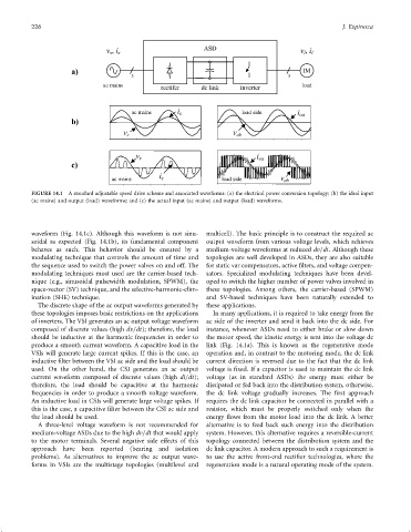
FIGURE 14.1 A standard adjustable speed drive scheme and associated waveforms: (a) the electrical power conversion topology; (b) the ideal input
(ac mains) and output (load) waveforms; and (c) the actual input (ac mains) and output (load) waveforms.
waveform (Fig. 14.1c). Although this waveform is not sinu- multicell). The basic principle is to construct the required ac
soidal as expected (Fig. 14.1b), its fundamental component output waveform from various voltage levels, which achieves
behaves as such. This behavior should be ensured by a medium-voltage waveforms at reduced dv=dt. Although these
modulating technique that controls the amount of time and topologies are well developed in ASDs, they are also suitable
the sequence used to switch the power valves on and off. The for static var compensators, active ®lters, and voltage compen-
modulating techniques most used are the carrier-based tech- sators. Specialized modulating techniques have been devel-
nique (e.g., sinusoidal pulsewidth modulation, SPWM), the oped to switch the higher number of power valves involved in
space-vector (SV) technique, and the selective-harmonic-elim- these topologies. Among others, the carrier-based (SPWM)
ination (SHE) technique. and SV-based techniques have been naturally extended to
The discrete shape of the ac output waveforms generated by these applications.
these topologies imposes basic restrictions on the applications In many applications, it is required to take energy from the
of inverters. The VSI generates an ac output voltage waveform ac side of the inverter and send it back into the dc side. For
composed of discrete values (high dv=dt); therefore, the load instance, whenever ASDs need to either brake or slow down
should be inductive at the harmonic frequencies in order to the motor speed, the kinetic energy is sent into the voltage dc
produce a smooth current waveform. A capacitive load in the link (Fig. 14.1a). This is known as the regenerative mode
VSIs will generate large current spikes. If this is the case, an operation and, in contrast to the motoring mode, the dc link
inductive ®lter between the VSI ac side and the load should be current direction is reversed due to the fact that the dc link
used. On the other hand, the CSI generates an ac output voltage is ®xed. If a capacitor is used to maintain the dc link
current waveform composed of discrete values (high di=dt); voltage (as in standard ASDs) the energy must either be
therefore, the load should be capacitive at the harmonic dissipated or fed back into the distribution system, otherwise,
frequencies in order to produce a smooth voltage waveform. the dc link voltage gradually increases. The ®rst approach
An inductive load in CSIs will generate large voltage spikes. If requires the dc link capacitor be connected in parallel with a
this is the case, a capacitive ®lter between the CSI ac side and resistor, which must be properly switched only when the
the load should be used. energy ¯ows from the motor load into the dc link. A better
A three-level voltage waveform is not recommended for alternative is to feed back such energy into the distribution
medium-voltage ASDs due to the high dv=dt that would apply system. However, this alternative requires a reversible-current
to the motor terminals. Several negative side effects of this topology connected between the distribution system and the
approach have been reported (bearing and isolation dc link capacitor. A modern approach to such a requirement is
problems). As alternatives to improve the ac output wave- to use the active front-end recti®er technologies, where the
forms in VSIs are the multistage topologies (multilevel and regeneration mode is a natural operating mode of the system.