
Page 146 - Science at the nanoscale
P. 146
8:11
RPS: PSP0007 - Science-at-Nanoscale
June 9, 2009
Low-Dimensional Nanostructures
136
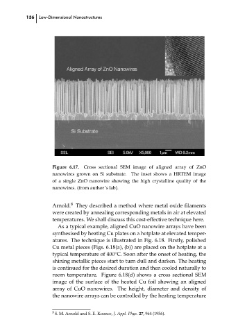
Cross sectional SEM image of aligned array of ZnO
Figure 6.17.
nanowires grown on Si substrate. The inset shows a HRTEM image
of a single ZnO nanowire showing the high crystalline quality of the
nanowires. (from author’s lab).
8
Arnold. They described a method where metal oxide filaments
were created by annealing corresponding metals in air at elevated
temperatures. We shall discuss this cost-effective technique here.
As a typical example, aligned CuO nanowire arrays have been
synthesised by heating Cu plates on a hotplate at elevated temper- ch06
atures. The technique is illustrated in Fig. 6.18. Firstly, polished
Cu metal pieces (Figs. 6.18(a), (b)) are placed on the hotplate at a
typical temperature of 400 C. Soon after the onset of heating, the
◦
shining metallic pieces start to turn dull and darken. The heating
is continued for the desired duration and then cooled naturally to
room temperature. Figure 6.18(d) shows a cross sectional SEM
image of the surface of the heated Cu foil showing an aligned
array of CuO nanowires. The height, diameter and density of
the nanowire arrays can be controlled by the heating temperature
8 S. M. Arnold and S. E. Koonce, J. Appl. Phys. 27, 964 (1956).