Page 129 - Semiconductor Manufacturing Handbook
P. 129

Geng(SMH)_CH10.qxd  04/04/2005  19:46  Page 10.2


                                       ION IMPLANTATION AND RAPID THERMAL PROCESSING

                   10.2  WAFER PROCESSING
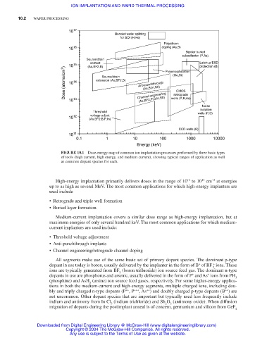
                                      10 17
                                                        Bonded wafer splitting
                                                          for SOI (H,He)
                                                                           Polysilicon
                                      10 16                               doping (As,B)
                                                                                   Bipolar buried
                                                                                  subcollector (P,As)
                                             Source/drain
                                               contact                                   Latchup/ESD
                                      10 15   (As,BF2,B)                    Preamorphization  protection (B)
                                     Dose (atoms/cm 2 )  10 14  extension (As,BF2,B)  Anti-punchthrough  (Ge,Si)
                                                   Source/drain
                                                                   (As,B,In,Sb)
                                                                                CMOS
                                                                               retrograde
                                                                 (As,BF2,P,B,In,Sb)
                                      10 13                      Channel engineering  wells (P,B,As)
                                                                                          Noise
                                                                                         isolation
                                                Threshold                               wells (P,B)
                                      10 12    voltage adjust
                                              (As,BF2,B,P,In)
                                                                                 CCD wells (B)
                                      10 11
                                         0.1         1         10        100        1000      10000
                                                                 Energy (keV)
                                    FIGURE 10.1  Dose-energy map of common ion implantation processes performed by three basic types
                                    of tools (high current, high energy, and medium current), showing typical ranges of application as well
                                    as common dopant species for each.


                                 High-energy implantation primarily delivers doses in the range of 10 to 10 cm at energies
                                                                                    11
                                                                                         13
                                                                                             −2
                               up to as high as several MeV. The most common applications for which high-energy implanters are
                               used include
                               • Retrograde and triple well formation
                               • Buried layer formation
                                 Medium-current implantation covers a similar dose range as high-energy implantation, but at
                               maximum energies of only several hundred keV. The most common applications for which medium-
                               current implanters are used include:

                               • Threshold voltage adjustment
                               • Anti-punchthrough implants
                               • Channel engineering/retrograde channel doping
                                 All segments make use of the same basic set of primary dopant species. The dominant p-type
                                                                                              +
                                                                                        +
                               dopant in use today is boron, usually delivered by the implanter in the form of B of BF ions. These
                                                                                              2
                               ions are typically generated from BF (boron trifluoride) ion source feed gas. The dominant n-type
                                                          3
                                                                                      +
                                                                                            +
                               dopants in use are phosphorus and arsenic, usually delivered in the form of P and As ions from PH 3
                               (phosphine) and AsH (arsine) ion source feed gases, respectively. For some higher-energy applica-
                                              3
                               tions in both the medium-current and high-energy segments, multiple charged ions, including dou-
                                                            ++
                                                                    ++
                                                                                                  ++
                               bly and triply charged n-type dopants (P , P +++ , As ) and doubly charged p-type dopants (B ) are
                               not uncommon. Other dopant species that are important but typically used less frequently include
                               indium and antimony from In Cl (indium trichloride) and Sb O (antimony oxide). When diffusion
                                                       3
                                                                             3
                                                                           2
                               migration of dopants during the postimplant anneal is of concern, germanium and silicon from GeF
                                                                                                      4
                          Downloaded from Digital Engineering Library @ McGraw-Hill (www.digitalengineeringlibrary.com)
                                     Copyright © 2004 The McGraw-Hill Companies. All rights reserved.
                                       Any use is subject to the Terms of Use as given at the website.
   124   125   126   127   128   129   130   131   132   133   134