
Page 407 - Sensors and Control Systems in Manufacturing
P. 407
Electric Field
Light entry side Industrial Sensors and Contr ol 361
p +
π A
p M
n
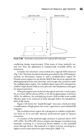
FIGURE 7.40 Schematic cross-section for a typical APD structure.
conflicting design requirements. What some of these tradeoffs are,
and how they are optimized in commercially available APDs, are
listed next.
Consider the schematic cross-section for a typical APD structure
(Fig. 7.40). The basic structural elements provided by the APD designer
include an absorption region A, and a multiplication region M.
Present across region A is an electric field E that serves to separate the
photogenerated holes and electrons, and sweeps one carrier towards
the multiplication region. The multiplication region M is designed to
exhibit a high electric field so as to provide internal photocurrent gain
by impact ionization.
This gain region must be broad enough to provide a useful gain,
M, of at least 100 for silicon APDs, or 10–40 for germanium or InGaAs
APDs. In addition, the multiplying electric field profile must enable
effective gain to be achieved at field strength below the breakdown
field of the diode.
Figure 7.40 shows the “reach-through” structure, which provides
a combination of high speed, low noise, capacitance, and extended IR
response.
The multiplication region M is designed to exhibit a high elec-
tric field so as to provide internal photocurrent gain by impact
ionization.
A variation of the reach-through structure is epitaxial silicon APD
(EPI-APD). The EPI-APD allows simpler and cheaper manufacturing
methods, resulting in a lower-cost device relative to the standard
reach-through device. The tradeoff is a higher k factor, resulting in a
higher excess noise factor for equivalent gain (Table 7.3).