
Page 145 - Six Sigma for electronics design and manufacturing
P. 145
Six Sigma for Electronics Design and Manufacturing
114
The following definitions apply to DPMO charts:
DPU = Defects found in PCB lot sample/total number of PCBs in
lot sample
MF = 1,000,000/total defect opportunities
DPMO = DPU × MF
D P M O = Average DPMO over time (20 samples minimum)
Control limits = D P M O ± 3 · D P M O /n u m b e r in l o t sa m p le
(U charts)
Control limits = D P M O ± 3 · D P M O (C charts)
Table 4.4 is an example of U chart DPMO-based calculations. The
DPMO chart is displayed in Figure 4.3. It is plotted by the daily activ-
ity of the assembly line for a particular PCB. The PCB was assembled
on different shifts and on different days by different operators. The
process seems to be out of control if two or more defects are found in
any point plots of the assembly line operation.
The control limits appear too narrow for the fluctuation of the pat-
tern, and the fluctuations are erratic. This called a pattern of instabil-
ity. Either more data is required for each DPMO point or the pattern
must be simplified before the data can be analyzed. Simplification
might involve some of the following steps:
Complex patterns might mean that the variable used as the basis
for plotting the point on the chart in sequence is not the most sig-
nificant variable. For example, the defects might vary according to
the shift or the operator manning the assembly line. The chart can
be replotted with the x axis data arranged according to these possi-
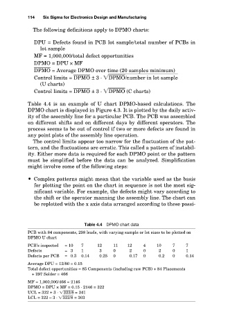
Table 4.4 DPMO chart data
PCB with 84 components, 298 leads, with varying sample or lot sizes to be plotted on
DPMO U chart
PCB’s inspected = 10 7 12 11 12 4 10 7 7
Defects = 3 1 3 0 2 0 2 0 1
Defects per PCB = 0.3 0.14 0.25 0 0.17 0 0.2 0 0.14
Average DPU = 12/80 = 0.15
Total defect opportunities = 85 Components (including raw PCB) + 84 Placements
+ 297 Solder = 466
MF = 1,000,000/466 = 2146
DPMO = DPU × MF = 0.15 · 2146 = 322
UCL = 322 + 3 · 3 2 2 /8 = 341
LCL = 322 – 3 · 3 2 2 /8 = 303