
Page 141 - Six Sigma for electronics design and manufacturing
P. 141
Six Sigma for Electronics Design and Manufacturing
110
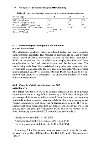
Table 4.2 Yield calculation in a line with n parts in a three-step production line
B
C
Process steps
A
Y(A)
Yield for each step
a
b
c
DPU at each process step
e
e
–na
–nc
e
Process yield (FTY) in each step
–nb
n
Or process yield (FTY) in each step
(1 – b)
(1 – a)
(1 – a)
Y{A}· Y{B}· Y{C}
Total process yield Y T
–n(a+b+c)
Or use FTY {total}
e
4.3.1 Determining first-time yield at the electronic Y(B) n Y(C) n
product turn-on level
The electronic products being developed today are more complex
than previous products. The number of components on each printed
circuit board (PCB) is increasing, as well as the total number of
PCBs in the product. In the following example, the effects of these
complexities on the final product turn-on will be demonstrated. The
historical quality level that sustained the production process for old-
er products is not adequate for new complex products. The in-process
manufacturing quality of components and PCBs will have to be im-
proved significantly to counteract the increased number of assem-
blies and components.
4.3.2 Example of yield calculations at the PCB
assembly level
The defect rate for new PCBs is usually calculated based on process
observations for existing PCBs. Assuming a PCB with through-hole
technology, defects are usually obtained from three sources: incoming
materials and components; assembly defects of missing, wrong, or re-
versed components; and soldering or termination defects. If it is as-
sumed that each component has 2.5 solder connections per PCB, the
quality level for multiple component PCBs can be calculated as fol-
lows, assuming reasonable PCB assembly process quality:
Solder defect rate DPU = 100 PPM
Component assembly defect rate DPU = 500 PPM
Incoming component defect rate DPU = 300 PPM
Assuming 2.5 solder connections per component, what is the total
process yield at the PCB test level for 100, 500, and 1000 component
PCBs?