
Page 1125 - The Mechatronics Handbook
P. 1125
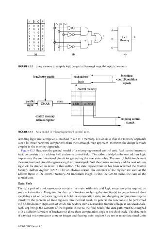
FIGURE 42.2  Using memory to simplify logic design: (a) Karnaugh map, (b) logic, (c) memory.


                                 FIGURE 42.3  Basic model of microprogrammed control units.

                                 decoding logic and storage cells involved in a 8 ×  1 memory, it is obvious that the memory approach
                                 uses a lot more hardware components than the Karnaugh map approach. However, the design is much
                                 simpler in the memory approach.
                                   Figure 42.3 illustrates the general model of a microprogrammed control unit. Each control memory
                                 location consists of an address field and some control fields. The address field plus the next address logic
                                 implements the combinational circuit for generating the next state value. The control fields implement
                                 the combinational circuit for generating the control signal. Both the control memory and the next address
                                 logic will be studied in detail in this section. The state register/counter has been renamed the Control
                                 Memory Address Register (CMAR) for an obvious reason: the contents of the register are used as the
                                 address input to the control memory. An important insight is that the CMAR stores the state of the
                                 control unit.
                                 Data Path
                                 The data path of a microprocessor contains the main arithmetic and logic execution units required to
                                 execute instructions. Designing the data path involves analyzing the function(s) to be performed, then
                                 specifying a set of hardware registers to hold the computation state, and designing computation steps to
                                 transform the contents of these registers into the final result. In general, the functions to be performed
                                 will be divided into steps, each of which can be done with a reasonable amount of logic in one clock cycle.
                                 Each step brings the contents of the registers closer to the final result. The data path must be equipped
                                 with a sufficient amount of hardware to allow these computation steps in one clock cycle. The data path
                                 of a typical microprocessor contains integer and floating-point register files, ten or more functional units


                                 ©2002 CRC Press LLC