
Page 1124 - The Mechatronics Handbook
P. 1124
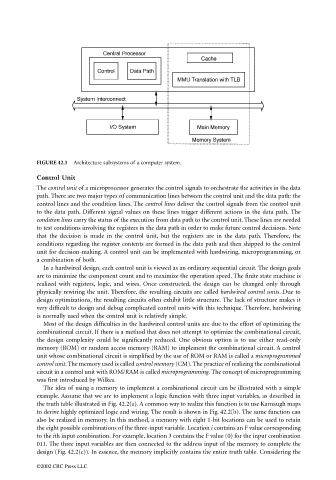
FIGURE 42.1  Architecture subsystems of a computer system.

                                 Control Unit
                                 The control unit of a microprocessor generates the control signals to orchestrate the activities in the data
                                 path. There are two major types of communication lines between the control unit and the data path: the
                                 control lines and the condition lines. The control lines deliver the control signals from the control unit
                                 to the data path. Different signal values on these lines trigger different actions in the data path. The
                                 condition lines carry the status of the execution from data path to the control unit. These lines are needed
                                 to test conditions involving the registers in the data path in order to make future control decisions. Note
                                 that the decision is made in the control unit, but the registers are in the data path. Therefore, the
                                 conditions regarding the register contents are formed in the data path and then shipped to the control
                                 unit for decision-making. A control unit can be implemented with hardwiring, microprogramming, or
                                 a combination of both.
                                   In a hardwired design, each control unit is viewed as an ordinary sequential circuit. The design goals
                                 are to minimize the component count and to maximize the operation speed. The finite state machine is
                                 realized with registers, logic, and wires. Once constructed, the design can be changed only through
                                 physically rewiring the unit. Therefore, the resulting circuits are called hardwired control units. Due to
                                 design optimizations, the resulting circuits often exhibit little structure. The lack of structure makes it
                                 very difficult to design and debug complicated control units with this technique. Therefore, hardwiring
                                 is normally used when the control unit is relatively simple.
                                   Most of the design difficulties in the hardwired control units are due to the effort of optimizing the
                                 combinational circuit. If there is a method that does not attempt to optimize the combinational circuit,
                                 the design complexity could be significantly reduced. One obvious option is to use either read-only
                                 memory (ROM) or random access memory (RAM) to implement the combinational circuit. A control
                                 unit whose combinational circuit is simplified by the use of ROM or RAM is called a microprogrammed
                                 control unit. The memory used is called control memory (CM). The practice of realizing the combinational
                                 circuit in a control unit with ROM/RAM is called microprogramming. The concept of microprogramming
                                 was first introduced by Wilkes.
                                   The idea of using a memory to implement a combinational circuit can be illustrated with a simple
                                 example. Assume that we are to implement a logic function with three input variables, as described in
                                 the truth table illustrated in Fig. 42.2(a). A common way to realize this function is to use Karnaugh maps
                                 to derive highly optimized logic and wiring. The result is shown in Fig. 42.2(b). The same function can
                                 also be realized in memory. In this method, a memory with eight 1-bit locations can be used to retain
                                 the eight possible combinations of the three-input variable. Location i contains an F value corresponding
                                 to the ith input combination. For example, location 3 contains the F value (0) for the input combination
                                 011. The three input variables are then connected to the address input of the memory to complete the
                                 design (Fig. 42.2(c)). In essence, the memory implicitly contains the entire truth table. Considering the

                                 ©2002 CRC Press LLC