
Page 1192 - The Mechatronics Handbook
P. 1192
Settling Time and Slew Rate
Settling time and slew rate together determine how rapidly a DAC can change the analog value it is out-
putting. Settling time refers to the amount of time it takes the output of the DAC to reach a specified
accuracy level. Most DACs specify settling time as a full-scale change in voltage, from the smallest output
value to the largest. Slew rate, specified in volt per second, is the maximum rate of change of the output
of the DAC. Therefore, a DAC with a fast slew rate and a small settling time can generate high-frequency
signals because an accurate voltage level can be obtained in a very small amount of time.
Offset Error and Gain Error
Offset error refers to the transfer characteristic of the DAC not outputting an analog value of 0 when
the digital value of 0 is applied. The range from zero to full would be offset from the specified value
because the offset would carry throughout the transfer function. The offset error can be thought of as a
translation in the transfer line either up or down from the ideal. Gain error indicates a linear deviation
from the ideal transfer line of a DAC. This can be caused by a variety of factors, which results in a change
of slope from the ideal.
Architecture of DACs
Unlike ADCs, DACs do not implement a wide range of approaches to convert a digital input code to an
analog value. Instead, almost all DACs use some combination of a switch network, resistive network, and
summing amplifier. This is not to say that all DACs have the same design, but they are all based on the
principle of switching.
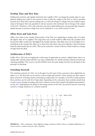
Switching Network
The switching network of a DAC can be thought of as the heart of the conversion. Since digital bits are
either on or off, these bits can be used to control single poll switches. These switches are then used to
direct some form of analog circuitry to develop an analog value. For example, a 3-bit DAC would comprise
three switches, one for each bit of input data. Depending on the code given, these switches would close
in such a way to develop an analog value from a reference source that is equal to the digital representation,
see Fig. 46.5. Depending on the design of the analog circuitry in the DAC, the switches may be connecting
current or voltage references to a resistive network.
FIGURE 46.5 DAC architecture—Most digital-to-analog converters (DACs) follow a standard architecture of a
switch network, a resistive network, and an amplifier.
©2002 CRC Press LLC