
Page 1190 - The Mechatronics Handbook
P. 1190
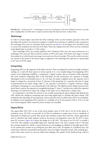
FIGURE 46.3  Multistage ADC—A multistage converter is a combination of the SAR and flash converters to provide
                                 faster sampling than the SARs and at a higher resolution than the flash converters could provide.
                                 Multistage

                                 In order to achieve higher rates than the SAR, multistage ADCs use the iterative approach of the SAR
                                 but reduce the number of comparisons needed to complete the conversion. In addition to the comparator,
                                 the multistage ADC uses low-resolution flash converters, see Fig 46.3. In the figure, the 6-bit flash is used
                                 to convert the residual errors from the 8-bit flash. These two outputs from the ADCs are then combined
                                 using digital logic to produce a 12-bit output.
                                   Most multistage ADCs are actually pipelined ADC. Pipelined ADCs have the same architecture as a
                                 multistage ADC, but each flash converter contains a T/H at the input. This allows each stage to convert
                                 the residual error while the previous stage has moved on to the next sample. This way the whole converter
                                 can operate at the speed of the slowest stage, as opposed to the multistage that operates at a speed equal
                                 to the sum of all the stages.


                                 Integrating
                                 Integrating ADCs are the opposite of the flash converter. They are designed to return very high-resolution
                                 reading. As a trade-off, they operate at slower speeds. It is a very simple design; the integrating ADCs
                                 consist of an integrating amplifier, a comparator, a digital counter, and an extremely stable capacitor.
                                 The most common integrating  ADC is the dual-slope. In this architecture, the capacitor is initially
                                 discharged to have no potential across it. At a set time, the input is applied across the capacitor and it
                                 begins to charge for a set period of time T 1 . Because of the properties of a capacitor, the rate of charge
                                 is proportional to the input voltage. After T 1 , the capacitor is switched to a negative reference voltage
                                 and begins to discharge at a rate proportional to the reference. The digital counter simply measures how
                                 much time it took for the capacitor to completely discharge T 2 . Since T 1  and the rate at which the capacitor
                                 discharges are both known values, the voltage of the input can be obtained by a simple ratio.
                                   It is important to note that the convert is not actually measuring the input voltage itself. Instead, the
                                 ADC obtains the voltage by measuring time and using digital logic to calculate the input voltage. This
                                 method has the advantage of rejecting noise, such as periodic noise, to which other ADCs are susceptible.
                                 In addition, most integrating ADCs operate on a multiple of an AC line period (1/60 or 1/50 s) so that
                                 stray electromagnetic fields caused by power systems are cancelled.

                                 Sigma-Delta
                                 The sigma-delta (SD) ADC is one of the most popular types of ADC due to its fit on the speed vs.
                                 resolution curve. SD ADCs can provide 16–24 bits of resolution at sample rates of up to hundreds of
                                 thousands of samples per second. This speed and resolution makes them ideal for certain applications
                                 such as vibration and audio analysis; however, the process of integration causes the SD ADC to have
                                 poor DC accuracy. Figure 46.4 shows the design of an SD ADC. The heart of an SD ADC is actually a
                                 1-bit ADC that samples at incredibly high rates. Typically, these 1-bit ADCs sample at 64 or 128 times
                                 the eventual sample rate, which is a process known as oversampling. In addition to the high-speed ADC,
                                 an SD architecture consists of an analog low-pass filter and a DAC all together in a feedback loop. The
                                 result forces otherwise unavoidable quantization noise into higher frequency bands. This resulting spec-
                                 trum of the noise is part of a process called noise shaping. The output of this feedback loop, which is

                                 ©2002 CRC Press LLC