
Page 272 - The Mechatronics Handbook
P. 272
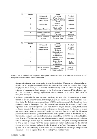
(a)     Levels                      Views
                                                                Behavioral     Structural    Physical
                                                      4        Performance   CPUs, Memory,   Physical
                                                              Specifications  Switches, Controllers,   Partitions
                                                                                 Buses
                                                      3        Algorithms      Modules,      Clusters
                                                                             Data Structures
                                                      2                       ALUs, MUXs,
                                                             Register Transfers             Floorplans
                                                                               Registers
                                                      1      Boolean Equations,  Gates,       Cells,
                                                                 FSMs          Flip-flops    Modules
                                                      0     Transfer Functions, Transistors, Wires,  Layout
                                                                 Timing      Contacts, Vias  Geometry

                                            (b)     Levels                      Views
                                                                Behavioral     Structural    Physical
                                                      4                        Sensors,      Physical
                                                               Performance     Actuators,
                                                              Specifications                 Partitions
                                                                               Systems
                                                      3                      Multiple Energy
                                                                                Domain       Clusters
                                                                              Components
                                                      2                      Domain-Domain  Floorplans
                                                                              Components
                                                      1                      Single Energy    Cells,
                                                                                Domain
                                                                              Components     Modules
                                                      0                         Beams,
                                                            Transfer Functions,  Membranes, Holes,  Layout
                                                                 Timing                     Geometry
                                                                             Grooves, Joints
                                 FIGURE 13.2 A taxonomy for component development (“levels and views”): (a) standard VLSI classifications,
                                 (b) a partial classification for MEMS components.

                                       A schematic diagram is an example of a structural description. Of course, not all circuit charac-
                                       teristics can be completely encapsulated in a single one of these views. For example, if we change
                                       the physical size of a wire, we will probably affect the timing, which is a behavioral property. The
                                       principle of encapsulation leads naturally to the development of extensive IP (intellectual prop-
                                       erty), i.e., libraries of increasingly sophisticated components that can be used as “black boxes” by
                                       the system developer.
                                     • Well-developed models for basic elements that clearly delineate effects due to changes in design,
                                       fabrication process, or environment. For example, in [10], the factors in the basic first-order equa-
                                       tions for I ds , the drain-to-source current in an NMOS transistor, can clearly be divided into those
                                       under the control of the designer (W/L, the width-to-length ratio for the transistor channel), those
                                       dependent on the fabrication process (ε, the permittivity of the gate insulator, and t ox , the thickness
                                       of the gate insulator), those dependent on environmental factors (V ds  and V gs , the drain-to-source
                                       and gate-to-source voltages, respectively), and those that are a function of both the fabrication
                                       process and the environment (µ, the effective surface mobility of the carriers in the channel, and V t ,
                                       the threshold voltage). More detailed information on modeling MOSFETs can be found in [11].
                                       Identification of fundamental parameters in one stage of the development process can be of great
                                       value in other stages. For example, the minimum feature size λ for a given technology can be used
                                       to develop a set of “design rules” that express mandatory overlaps and spacings for the different
                                       physical materials. A design tool can then be developed to “enforce” these rules, and the conse-
                                       quences can be used to simplify, to some extent, the modeling and simulation stages. The parameter
                                       λ can also be used to express effects due to scaling when scaling is valid.

                                 ©2002 CRC Press LLC