
Page 273 - The Mechatronics Handbook
P. 273
• Mature tools for design and simulation, which have evolved over many generations and for which
moderately priced versions are available from multiple sources. For example, many of today’s tools
incorporate versions of the design tool MAGIC [12] and the simulator SPICE (Simulation Program
with Integrated Circuit Emphasis) [13], both of which were originally developed at the University
of California, Berkeley. Versions of the SPICE simulator typically support several device models
(currently, for example, six or more different MOS models and five different transmission line
models), so that a developer can choose the level of device detail appropriate to the task at hand.
Free or low-cost versions of both MAGIC and SPICE, as well as extended versions of both tools, are
widely available. Many different techniques, such as model binning (optimizing models for specific
ranges of model parameters) and inclusion of proprietary process information, are employed to
produce better models and simulation results, especially in the HSPICE version of SPICE and in
other high-end versions of these tools [11].
• Integrated development systems that are widely available and that provide support for a variety
of levels and views, extensive component libraries, user-friendly interfaces and online help, as well
as automatic translation between domains, along with error and constraint checking. In an inte-
grated VLSI development system, sophisticated models, simulators, and translators keep track of
circuit information for multiple levels and views, while allowing the developer to focus on one
level or view at a time. Many development systems available today also support, at the higher
levels of abstraction, structured “programming” languages such as VHDL (Very Large Scale Inte-
grated Circuit Hardware Description Language) [14,15] or Verilog [16].
A digital circuit developer has many options, depending on performance constraints, number of units
to be produced, desired cost, available development time, etc. At one extreme the designer may choose
to develop a “custom” circuit, creating layout geometries, sizing individual transistors, modeling RC
effects in individual wires, and validating design choices through extensive low-level SPICE-based sim-
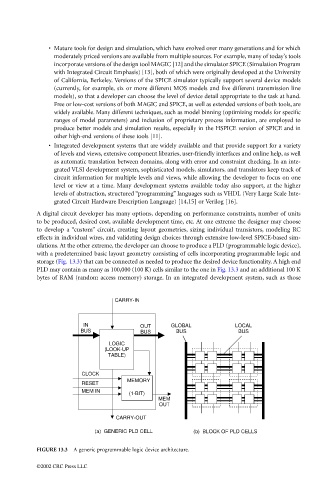
ulations. At the other extreme, the developer can choose to produce a PLD (programmable logic device),
with a predetermined basic layout geometry consisting of cells incorporating programmable logic and
storage (Fig. 13.3) that can be connected as needed to produce the desired device functionality. A high end
PLD may contain as many as 100,000 (100 K) cells similar to the one in Fig. 13.3 and an additional 100 K
bytes of RAM (random access memory) storage. In an integrated development system, such as those
CARRY-IN
IN OUT GLOBAL LOCAL
BUS BUS BUS BUS
LOGIC
(LOOK-UP
TABLE)
CLOCK
MEMORY
RESET
MEM IN
(1-BIT)
MEM
OUT
CARRY-OUT
(a) GENERIC PLD CELL (b) BLOCK OF PLD CELLS
FIGURE 13.3 A generic programmable logic device architecture.
©2002 CRC Press LLC