Page 274 - The Mechatronics Handbook
P. 274

provided by [17] and [18], the developer enters the design in either schematic form or a high level
                                 language, and then the design is automatically  “compiled” and mapped to the PLD geometry, and
                                 functional and timing simulations can be run. If the simulation results are acceptable, an actual PLD can
                                 then be programmed directly, as a further step in the development process, and even tested, to some
                                 extent, with the same set of test data as was used for the simulation step. This “rapid prototyping” [19]
                                 for the production of a “chip” is not very different from the production of a working software program
                                 (and the PLD can be reprogrammed if different functionality is later desired). Such a system, of course,
                                 places many constraints on achievable designs. In addition, the automated steps, which rely on heuristics
                                 rather than exact techniques to find acceptable solutions to the many computationally complex problems
                                 that need to be solved during the development process, sacrifice performance for ease of development,
                                 so that a device designed in such a system will never achieve the ultimate performance possible for the
                                 given technology. However, the trade-offs include ease of use, much shorter development times, and the
                                 management of much larger numbers of individual circuit elements than would be possible if each
                                 individual element were tuned to its optimum performance. In addition, if a high-level language is used
                                 for input, an acceptable design can often be translated, with few changes, to a more powerful design
                                 system that will allow implementation in more flexible technologies and additional fine tuning of circuit
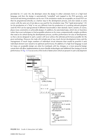
                                 performance. In Fig. 13.4 we see some of the levels of abstraction which are present in such a development


                                                  TRANSISTOR
                                                     (PHYSICAL VIEW)


                                                         LIBRARY
                                                         COMPONENT
                                                           (PHYS. / BEHAV./
                                                                 STRUCT.)


                                                                 NETLIST
                                                                    (STRUCTURAL)
                                                                 n1:  a  b  o1

                                                                 n2:  a   c  o2
                                                                           VHDL
                                                                 n3:  o1  o2  o3
                                                                           entity HALFADDER is
                                                                             port (A,B: in bit;
                                                                                     S,COUT: out bit);
                                                                           end ADDER;
                                                                           architecture A of HALFADDER is
                                                                             component XOR
                                                                                port (X1,X2: in bit; O: out bit);
                                                                             end component;
                                                                             component AND
                                                                                port (X1,X2: in bit; O: out bit);
                                                                             end component;
                                                                             begin
                                                                                G1: XOR
                                                                                   port map (A,B,S);
                                                                                G2:  AND
                                                                                   Port map (A,B,COUT);
                                                                             end A;


                                 FIGURE 13.4  Levels of abstraction–half adder.

                                 ©2002 CRC Press LLC
   269   270   271   272   273   274   275   276   277   278   279