
Page 659 - The Mechatronics Handbook
P. 659
0066_Frame_C20.fm Page 129 Wednesday, January 9, 2002 1:48 PM
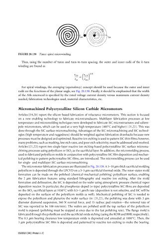
r (θ)
r (θ)
r IR
r IR
r OR r OR
FIGURE 20.138 Planar spiral microwinding.
Thus, using the number of turns and turn-to-turn spacing, the outer and inner radii of the k-turn
winding are found as
------- = r OR 1/N
r Ok
-------
r Ik r IR
For spiral windings, the averaging (equivalency) concept should be used because the outer and inner
radii are the functions of the planar angle, see Fig. 20.138. Finally, it should be emphasized that the width
of the Nth microcoil is specified by the rated voltage current density versus maximum current density
needed, fabrication technologies used, material characteristics, etc.
Micromachined Polycrystalline Silicon Carbide Micromotors
Articles [19,20] report the silicon-based fabrication of reluctance micromotors. This section is focused
on a new enabling technology to fabricate microtransducers. Multilayer fabrication processes at low
temperature and micromolding techniques were developed to fabricate SiC microstructures and salient-
pole micromotors, which can be used at a very high temperature (400°C and higher) [21,22]. This was
done through the SiC surface micromachining. Advantages of the SiC micromachining and SiC technol-
ogies (high temperature and ruggedness) should be weighted against fabrication drawbacks because new
processes must be designed and optimized. Reactive ion etching is used to pattern SiC thin films; however,
many problems, such as masking, low etch rates, and poor etch selectivity, must be addressed and resolved.
Articles [21,22] report two single-layer reactive ion etching-based polycrystalline SiC surface microma-
chining processes using polysilicon or SiO 2 as the sacrificial layer. In addition, the micromolding process,
used to fabricated polysilicon molds in conjunction with polycrystalline SiC film deposition and mechan-
ical polishing to pattern polycrystaline SiC films, are introduced. The micromolding process can be used
for single- and multilayer SiC surface micromachining.
The micromotor fabrication processes are illustrated in Fig. 20.139. A 5–10 µm thick sacrificial molding
polysilicon is deposited through the LPCVD on a 3–5 µm sacrificial thermal oxide. The rotor-stator mold
formation can be made on the polished (chemical-mechanical polishing) polysilicon surface, enabling
the 2 µm fabrication features using standard lithography and reactive ion etching. After the mold
formation and delineation, the SiC is deposited on the wafer using atmospheric pressure chemical vapor
deposition reactor. In particular, the phosphorus-doped (n-type) polycrystalline SiC films are deposited
on the SiO 2 sacrificial layers at 1050°C with 0.5–1 µm/h rate (deposition is not selective, and SiC will be
deposited on the surfaces of the polysilicon molds as well). Mechanical polishing of SiC is needed to
expose the polysilicon and planarize the wafer surface (in [21,22], the polishing was done with 3 µm
diameter diamond suspension, 360 N normal force, and 15 rad/sec pad rotation—the removal rate of
SiC was reported to be 100 nm/min). The wafers are polished until the top surface of the polysilicon
mold is exposed (polishing must be stopped at once due to the fast polishing rate). The flange mold is
fabricated through the polysilicon and the sacrificial oxide etching (using the KOH and BHF, respectively).
The 0.5 µm bearing clearance low-temperature oxide is deposited and annealed at 1000°C. Then, the
1 µm polycrystalline SiC film is deposited and patterned by reactive ion etching to make the bearing.
©2002 CRC Press LLC