
Page 150 - ARM Based Microcontroller Projects Using MBED
P. 150
136 8. INTERMEDIATE LEVEL PROJECTS
FIG. 8.1 Block diagram of the project.
8.2.4 Circuit Diagram
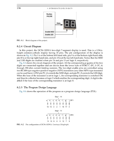
In this project, the DC56-11EWA two-digit 7-segment display is used. This is a 0.56in.
height common-cathode display having 18 pins. The pin configuration of the display is
shown in Fig. 8.2. Pin 1 is at the bottom left-hand side, pin 9 is at the bottom right-hand side,
pin 10 is at the top right-hand side, and pin 18 is at the top left-hand side. Notice that the MSD
and LSD digits are enabled when pin 14 and pin 13 are logic 0, respectively.
Fig. 8.3 shows the circuit diagram of the project. All the corresponding a–g pins of the two
digits are connected together and are driven from the lower byte of PORT C (PC_0–PC_6)
through 390 ohm current limiting resistors. The two-digit enable pins are controlled using
two BC108-type negative-positive-negative (NPN) transistors (any other NPN-type transistor
can be used here). GPIO pin PC_8 controls the MSD digit, and pin PC_9 controls the LSD digit.
When the base of the transistor is set to logic 1, the corresponding transistor is switched ON
and thus its collector becomes at logic 0 which enables the corresponding digit. A digit is dis-
abled if the base of the corresponding transistor is at logic 0.
8.2.5 The Program Design Language
Fig. 8.4 shows the operation of the program as a program design language (PDL).
Dig1 : 14
a b c d e f g DP1
16 15 3 2 1 18 17 4
Dig2 : 13
a b c d e f g DP2
11 10 8 6 5 12 7 9
FIG. 8.2 Pin configuration of DC56-11EWA. Courtesy of Kingbright.