
Page 150 - An Introduction to Microelectromechanical Systems Engineering
P. 150
Summary 129
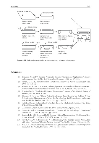
Silicon nitride
Silicon dioxide
Pattern oxide Etch grooves;
and nitride strip nitride
Silicon nitride
p+ Si
Pattern front side Etch grooves; Etch from back side;
nitride pattern back side stop on p+;
nitride strip nitride
Silicon nitride p+ Si Silicon nitride
Pattern nitride; Protect front side; RIE p+ Si;
etch shallow pattern back side; strip nitride
grooves etch cavities;
stop on p+.
Figure 4.38 Fabrication process for an electrostatically actuated micropump.
References
[1] Yamazoe, N., and Y. Shimizu, “Humidity Sensors: Principles and Applications,” Sensors
and Actuators, Vol. 10, No. 3–4, November–December 1986, pp. 379–398.
[2] Kovacs, G. T. A., Micromachined Transducers Sourcebook, New York: McGraw-Hill,
1998, pp. 614–623.
[3] Johnson, W. A., and L. K. Warne, “Electrophysics of Micromechanical Comb Actuators,”
Journal of Microelectromechanical Systems, Vol. 4, No. 1, March 1995, pp. 49–59.
[4] Timoshenko, S., “Analysis of Bi-Metal Thermostats,” Journal of the Optical Society of
America, Vol. 11, 1925, p. 233.
[5] Klaassen, E. H., et al., “Silicon Fusion Bonding and Deep Reactive Ion Etching; A New
Technology for Microstructures,” Proc. 8th Int. Conf. on Solid-State Sensors and Actua-
tors, Stockholm, Sweden, June 25–29, 1995, pp. 556–559.
[6] Halliday, D., and R. Resnick, Physics, Part Two, 3rd ed., Extended version, New York:
Wiley, 1986, pp. 718–724.
[7] U.S. Patents 3,921,916, November 25, 1975, and 3,949,410, April 6, 1976.
[8] Peeters, E., and S. Verdonckt-Vandebroek, “Thermal Ink Jet Technology,” Circuits and
Devices, Vol. 13, No. 4, July 1997, pp. 19–23.
[9] Kneisel, L. L., J. D. Baker, and L. N. Goenka, “Silicon Micromachined CO Cleaning Noz-
2
zle and Method,” U.S. Patent 5,545,073, August 13, 1996.
[10] Siewell, G. L., W. R. Boucher, and P. H. McClelland, “The ThinkJet Orifice Plate: A Part
with Many Functions,” Hewlett-Packard Journal, Vol. 36, No. 5, May 1985, pp. 33–37.
[11] Wu, M. C., “Micromachining for Optical and Optoelectronic Systems,” Proceedings of the
IEEE, Vol. 85, No. 11, November 1997, pp. 1833–1856.