
Page 155 - An Introduction to Microelectromechanical Systems Engineering
P. 155
134 MEM Structures and Systems in Photonic Applications
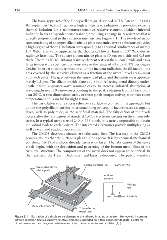
The basic approach of the Honeywell design, described in U.S. Patent 6,621,083
B2 (September 16, 2003), achieves high sensitivity to radiation by providing extreme
thermal isolation for a temperature-sensitive resistive element. Incident infrared
radiation heats a suspended sense resistor, producing a change in its resistance that is
directly proportional to the radiation intensity (see Figure 5.1). The two-level struc-
ture, consisting of an upper silicon nitride plate suspended over a substrate, provides
a high degree of thermal isolation corresponding to a thermal conductance of merely
10 W/K. This value approaches the theoretical lowest limit of 10 W/K due to
-8
-9
radiative heat loss. The square silicon nitride plate is 50 µm on a side and 0.5 µm
thick. The thin (50- to 100-nm) resistive element rests on the silicon nitride and has a
large temperature coefficient of resistance in the range of –0.2 to –0.3% per degree
Celsius. In order to capture most or all of the incident radiation, the fill factor—the
area covered by the sensitive element as a fraction of the overall pixel area—must
approach unity. The gap between the suspended plate and the substrate is approxi-
mately 1.8 µm. The silicon nitride plate and a thin reflecting metal directly under-
neath it form a quarter-wave resonant cavity to increase infrared absorption at
wavelengths near 10 µm—corresponding to the peak radiation from a black body
near 20ºC. A two-dimensional array of these pixels images activity at or near room
temperature and is useful for night vision.
The basic fabrication process relies on a surface micromachining approach, but
unlike the polysilicon surface micromachining process, it incorporates an organic
layer, such as polyimide, as the sacrificial material. The fabrication of the pixels
occurs after the fabrication of standard CMOS electronic circuits on the silicon sub-
strate. In a typical array size of 240 × 336 pixels, it is nearly impossible to obtain
individual leads to each element. The integrated electronics provide multiplexing as
well as scan and readout operations.
The CMOS electronic circuits are fabricated first. The last step in the CMOS
process ensures that the surface is planar. One approach is by chemical-mechanical
polishing (CMP) of a silicon dioxide passivation layer. The fabrication of the sense
pixels begins with the deposition and patterning of the bottom metal films of the
two-level structure. The composition of the metal does not appear to be critical. In
the next step, the 1.8-µm thick sacrificial layer is deposited. The public literature
Resistive element (TCR ~ − 0.2% per ºC)
Suspended silicon
nitride plate
Address
column
Address
row
R
Substrate
Metal interconnect
Thin reflecting
metal layer
Figure 5.1 Illustration of a single sense element in the infrared imaging array from Honeywell. Incoming
infrared radiation heats a sensitive resistive element suspended on a thin silicon nitride plate. Electronic
circuits measure the change in resistance and infer the radiation intensity. (After: [1].)