
Page 157 - An Introduction to Microelectromechanical Systems Engineering
P. 157
136 MEM Structures and Systems in Photonic Applications
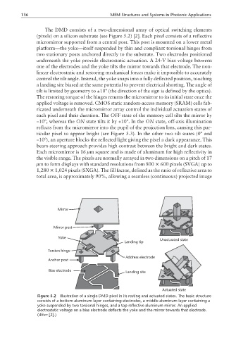
The DMD consists of a two-dimensional array of optical switching elements
(pixels) on a silicon substrate (see Figure 5.2) [2]. Each pixel consists of a reflective
micromirror supported from a central post. This post is mounted on a lower metal
platform—the yoke—itself suspended by thin and compliant torsional hinges from
two stationary posts anchored directly to the substrate. Two electrodes positioned
underneath the yoke provide electrostatic actuation. A 24-V bias voltage between
one of the electrodes and the yoke tilts the mirror towards that electrode. The non-
linear electrostatic and restoring mechanical forces make it impossible to accurately
control the tilt angle. Instead, the yoke snaps into a fully deflected position, touching
a landing site biased at the same potential to prevent electrical shorting. The angle of
tilt is limited by geometry to ±10º (the direction of the sign is defined by the optics).
The restoring torque of the hinges returns the micromirror to its initial state once the
applied voltage is removed. CMOS static random-access memory (SRAM) cells fab-
ricated underneath the micromirror array control the individual actuation states of
each pixel and their duration. The OFF state of the memory cell tilts the mirror by
–10º, whereas the ON state tilts it by +10º. In the ON state, off-axis illumination
reflects from the micromirror into the pupil of the projection lens, causing this par-
ticular pixel to appear bright (see Figure 5.3). In the other two tilt states (0º and
–10º), an aperture blocks the reflected light giving the pixel a dark appearance. This
beam-steering approach provides high contrast between the bright and dark states.
Each micromirror is 16 µm square and is made of aluminum for high reflectivity in
the visible range. The pixels are normally arrayed in two dimensions on a pitch of 17
µm to form displays with standard resolutions from 800 × 600 pixels (SVGA) up to
1,280 × 1,024 pixels (SXGA). The fill factor, defined as the ratio of reflective area to
total area, is approximately 90%, allowing a seamless (continuous) projected image
Mirror
Mirror post
Yoke Unactuated state
Landing tip
Torsion hinge
Address electrode
Anchor post
Bias electrode Landing site
Actuated state
Figure 5.2 Illustration of a single DMD pixel in its resting and actuated states. The basic structure
consists of a bottom aluminum layer containing electrodes, a middle aluminum layer containing a
yoke suspended by two torsional hinges, and a top reflective aluminum mirror. An applied
electrostatic voltage on a bias electrode deflects the yoke and the mirror towards that electrode.
(After: [2].)