
Page 158 - An Introduction to Microelectromechanical Systems Engineering
P. 158
Imaging and Displays 137
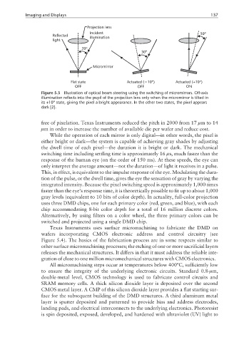
Projection lens
Incident 10º
Reflected illumination
light
20º
30º
Micromirror
−
Flat state Actuated ( 10º) Actuated (+10º)
OFF OFF ON
Figure 5.3 Illustration of optical beam steering using the switching of micromirrors. Off-axis
illumination reflects into the pupil of the projection lens only when the micromirror is tilted in
its +10º state, giving the pixel a bright appearance. In the other two states, the pixel appears
dark [2].
free of pixelation. Texas Instruments reduced the pitch in 2000 from 17 µmto14
µm in order to increase the number of available die per wafer and reduce cost.
While the operation of each mirror is only digital—in other words, the pixel is
either bright or dark—the system is capable of achieving gray shades by adjusting
the dwell time of each pixel—the duration it is bright or dark. The mechanical
switching time including settling time is approximately 16 µs, much faster than the
response of the human eye (on the order of 150 ms). At these speeds, the eye can
only interpret the average amount—not the duration—of light it receives in a pulse.
This, in effect, is equivalent to the impulse response of the eye. Modulating the dura-
tion of the pulse, or the dwell time, gives the eye the sensation of gray by varying the
integrated intensity. Because the pixel switching speed is approximately 1,000 times
faster than the eye’s response time, it is theoretically possible to fit up to about 1,000
gray levels (equivalent to 10 bits of color depth). In actuality, full-color projection
uses three DMD chips, one for each primary color (red, green, and blue), with each
chip accommodating 8-bit color depth for a total of 16 million discrete colors.
Alternatively, by using filters on a color wheel, the three primary colors can be
switched and projected using a single DMD chip.
Texas Instruments uses surface micromachining to fabricate the DMD on
wafers incorporating CMOS electronic address and control circuitry (see
Figure 5.4). The basics of the fabrication process are in some respects similar to
other surface micromachining processes; the etching of one or more sacrificial layers
releases the mechanical structures. It differs in that it must address the reliable inte-
gration of close to one million micromechanical structures with CMOS electronics.
All micromachining steps occur at temperatures below 400ºC, sufficiently low
to ensure the integrity of the underlying electronic circuits. Standard 0.8-µm,
double-metal level, CMOS technology is used to fabricate control circuits and
SRAM memory cells. A thick silicon dioxide layer is deposited over the second
CMOS metal layer. A CMP of this silicon dioxide layer provides a flat starting sur-
face for the subsequent building of the DMD structures. A third aluminum metal
layer is sputter deposited and patterned to provide bias and address electrodes,
landing pads, and electrical interconnects to the underlying electronics. Photoresist
is spin deposited, exposed, developed, and hardened with ultraviolet (UV) light to