
Page 258 - An Introduction to Microelectromechanical Systems Engineering
P. 258
Types of Packaging Solutions 237
Gel Thick-film
resistor
Plastic cap
Ceramic
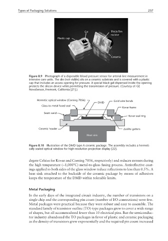
Figure 8.9 Photograph of a disposable blood pressure sensor for arterial-line measurement in
intensive care units. The die (not visible) sits on a ceramic substrate and is covered with a plastic
cap that includes an access opening for pressure. A special black gel dispensed inside the opening
protects the silicon device while permitting the transmission of pressure. (Courtesy of: GE
NovaSensor, Fremont, California [21].)
Hermetic optical window (Corning 7056) Gold wire bonds
DMD
Glass-to-metal fused seal
Kovar frame
Seam weld
Kovar seal ring
Ceramic header Zeolite getters
Heat sink
Figure 8.10 Illustration of the DMD type-A ceramic package. The assembly includes a hermeti-
cally sealed optical window for high-resolution projection display [22].
degree Celsius for Kovar and Corning 7056, respectively) and reduces stresses during
the high temperature (~1,000ºC) metal-to-glass fusing process. Antireflective coat-
ings applied to both sides of the glass window reduce reflections to less than 0.5%. A
heat sink attached to the backside of the ceramic package by means of adhesives
keeps the temperature of the DMD within tolerable limits.
Metal Packaging
In the early days of the integrated circuit industry, the number of transistors on a
single chip and the corresponding pin count (number of I/O connections) were few.
Metal packages were practical because they were robust and easy to assemble. The
standard family of transistor outline (TO)-type packages grew to cover a wide range
of shapes, but all accommodated fewer than 10 electrical pins. But the semiconduc-
tor industry abandoned the TO packages in favor of plastic and ceramic packaging
as the density of transistors grew exponentially and the required pin count increased