
Page 257 - An Introduction to Microelectromechanical Systems Engineering
P. 257
236 Packaging and Reliability Considerations for MEMS
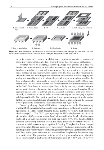
1. Cast ceramic 2. Punch holes 3. Fill 4. Metallize 5. Cut, stack, and laminate
tape
9. Gold or nickel plate 8. Braze pins 7. Nickel plate 6. Sinter
Figure 8.8 Process flow for the fabrication of a cofired laminated ceramic package with electrical pins and
access ports. (Courtesy of: the Coors Electronic Package Company of Golden, Colorado.)
attractive feature of ceramic is the ability to screen print on its surface a network of
thick-film resistors that can be later trimmed with a laser for sensor calibration.
Whether custom or standard, a ceramic package often consists of a base or a
header onto which one die or many dice are attached by adhesives or solder. Wire
bonding is suitable for electrical interconnects. Flip-chip bonding to a pattern of
metal contacts on the ceramic works equally well. The final step after mounting the
die on the base and providing suitable electrical interconnects involves capping and
sealing the assembly with a lid whose shape and properties are determined by the
final application. For instance, the lid must be transparent for optical MEMS or must
hermetically seal a vacuum, as is the case for the infrared bolometer from Honeywell
or the DMD from Texas Instruments (see Chapter 5). By contrast, a plastic cover pro-
vides a cost-effective solution for low-cost devices. For example, disposable blood
pressure sensors used for arterial-line measurement in intensive care units are pro-
tected by a plastic cover that includes an access opening for pressure [21]. A special
gel dispensed inside this opening provides limited protection (particularly against
biological solutions and electrical charge) to the device while permitting the transmis-
sion of pressure to the sensitive silicon membrane (see Figure 8.9).
Ceramic packaging of optical MEMS can be complex and costly. This is certainly
true for DMD packages that have undergone a continuous evolution from their early
application in airline ticket boarding (ATB) printers to today’s high-resolution
display arrays [22]. The DMD type-A package for SVGA displays consists of a 114-
pin alumina (Al O ) ceramic header (base) with metallization for electrical intercon-
2 3
nects and a Cu-Ag brazed Kovar seal ring (see Figure 8.10). Wire bonds establish
electrical connectivity between the die and metal traces on the ceramic header. A
transparent window consisting of a polished Corning 7056 glass fused to a stamped
gold-nickel-plated Kovar frame covers the assembly. Resistance seam welding of the
seal ring on the ceramic base to the Kovar glass frame provides a permanent hermetic
seal. Two zeolite getter strips attached to the inside of the glass window ensure long-
term desiccation. The particular choice of metal and glass window materials mini-
−6
mizes the mismatch in coefficients of thermal expansion (4 × 10 and 5 × 10 −6 per