
Page 256 - An Introduction to Microelectromechanical Systems Engineering
P. 256
Types of Packaging Solutions 235
packages such as ball grid arrays (BGA) [20]. These same characteristics have
extended the utility of ceramics to the packaging of MEMS—many commercially
available micromachined sensors use some form of ceramic packaging. Ceramics
are completely customizable and allow the formation of through ports and mani-
folds for the packaging of fluid-based MEMS. Ceramics usually suffer from shrink-
age (~13% in the horizontal direction and ~15% in the vertical direction) during
firing, which manufacturers take into account in their designs. Compared to plastic
packaging, they are significantly more expensive.
Alumina (Al O ) is by far the most common of all ceramics, having been used
2 3
over the centuries in porcelain and fine dinnerware. Aluminum nitride (AlN) and
beryllia (BeO) have superior material properties (e.g., better thermal conductivity),
but the latter is very toxic. Aluminum nitride substrates tend to be costly in particu-
lar because of required complex processing due to the difficulty of sintering the
material.
A ceramic package is made of laminates, each formed and patterned separately,
then brought together and cofired (sintered) at an elevated temperature—typically
between 1,500ºC and 1,600ºC (see Figure 8.8). Recent advances have led to low-
temperature cofired ceramics (LTCC), such as the Dupont 951 Green Tape™, with
sintering temperatures near 800ºC. Powders are first mixed together with special
additives and extruded under a knife edge to form a thin laminate sheet. This
“green” unfired soft tape, approximately 0.1 to 0.3 mm thick, is peeled from the
supporting table, then cut and punched using precise machining tools. Patterns of
electrical interconnects are screen printed on each sheet using a slurry of tungsten
powder or tungsten-molybdenum. This process also fills via holes with metal. Vias
left unfilled with tungsten can be later used as fluid- or pressure-access ports
through the ceramic. Several “green” sheets are aligned and press laminated
together, then cofired at an elevated temperature in a reducing atmosphere to sinter
the laminate stack into a monolithic body. A typical integrated circuit package con-
sists of three laminates, but as many as sixteen may be simultaneously cofired, natu-
rally at a higher material cost. An appropriate metal finish is then applied to the
tungsten, followed by plating of nickel. If necessary, pins or leads are brazed to the
package. The leads are typically made of ASTM F-15 alloy (also known as Kovar ,
it is an alloy that consists of 52% iron, 29% nickel, and 18% cobalt) that has a ther-
mal expansion coefficient matched to that of alumina. The brazing material is often
a silver-copper eutectic alloy. A final nickel and electroless gold-plating step ensures
that wires can be bonded to the leads. A BGA ceramic package has no pins brazed;
rather, it has arrays of solder balls connected to electrical feed throughs. One
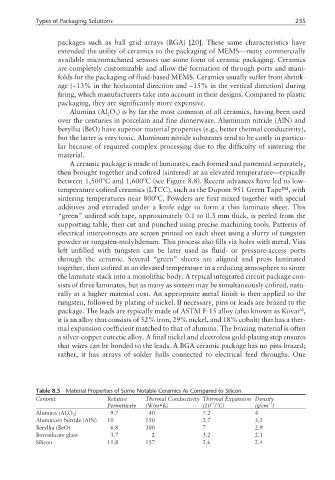
Table 8.5 Material Properties of Some Notable Ceramics As Compared to Silicon
Ceramic Relative Thermal Conductivity Thermal Expansion Density
−6
−3
Permittivity (W/m•K) (10 /ºC) (g/cm )
Alumina (Al O ) 09.7 040 7.2 4
3
2
Aluminum Nitride (AlN) 10 150 2.7 3.2
Beryllia (BeO) 06.8 300 7 2.9
Borosilicate glass 03.7 002 3.2 2.1
Silicon 11.8 157 2.6 2.4