
Page 251 - An Introduction to Microelectromechanical Systems Engineering
P. 251
230 Packaging and Reliability Considerations for MEMS
Silicon substrate
Silicon oxide
SiN Bondpad metal
Titanium
Sputtered Cu
Plated Cu
Plated solder
IC or MEMS die
Solder paste
Conductor
Bondpad Solder
bump
Dielectric layers
Metal interconnect layers
Package substrate
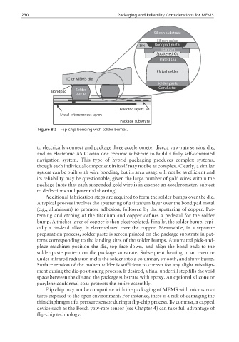
Figure 8.5 Flip-chip bonding with solder bumps.
to electrically connect and package three accelerometer dice, a yaw-rate sensing die,
and an electronic ASIC onto one ceramic substrate to build a fully self-contained
navigation system. This type of hybrid packaging produces complex systems,
though each individual component in itself may not be as complex. Clearly, a similar
system can be built with wire bonding, but its area usage will not be as efficient and
its reliability may be questionable, given the large number of gold wires within the
package (note that each suspended gold wire is in essence an accelerometer, subject
to deflections and potential shorting).
Additional fabrication steps are required to form the solder bumps over the die.
A typical process involves the sputtering of a titanium layer over the bond pad metal
(e.g., aluminum) to promote adhesion, followed by the sputtering of copper. Pat-
terning and etching of the titanium and copper defines a pedestal for the solder
bump. A thicker layer of copper is then electroplated. Finally, the solder bump, typi-
cally a tin-lead alloy, is electroplated over the copper. Meanwhile, in a separate
preparation process, solder paste is screen printed on the package substrate in pat-
terns corresponding to the landing sites of the solder bumps. Automated pick-and-
place machines position the die, top face down, and align the bond pads to the
solder-paste pattern on the package substrate. Subsequent heating in an oven or
under infrared radiation melts the solder into a columnar, smooth, and shiny bump.
Surface tension of the molten solder is sufficient to correct for any slight misalign-
ment during the die-positioning process. If desired, a final underfill step fills the void
space between the die and the package substrate with epoxy. An optional silicone or
parylene conformal coat protects the entire assembly.
Flip chip may not be compatible with the packaging of MEMS with microstruc-
tures exposed to the open environment. For instance, there is a risk of damaging the
thin diaphragm of a pressure sensor during a flip-chip process. By contrast, a capped
device such as the Bosch yaw-rate sensor (see Chapter 4) can take full advantage of
flip-chip technology.