
Page 250 - An Introduction to Microelectromechanical Systems Engineering
P. 250
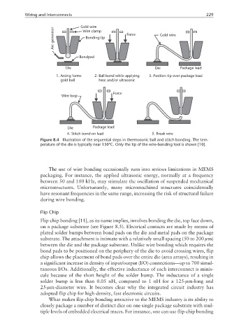
Wiring and Interconnects                                                      229

                                    Gold wire
                        generator    Wire clamp        Force          Gold wire
                                      Bonding tip
                        Arc

                                   Bondpad

                             Die                                    Die        Package lead
                         1. Arcing forms  2. Ball bond while applying  3. Position tip over package lead
                           gold ball       heat and/or ultrasonic


                                                  Force
                           Wire loop


                              Die        Package lead
                              4. Stitch bond on lead              5. Break wire
                  Figure 8.4  Illustration of the sequential steps in thermosonic ball and stitch bonding. The tem-
                  perature of the die is typically near 150ºC. Only the tip of the wire-bonding tool is shown [10].


                      The use of wire bonding occasionally runs into serious limitations in MEMS
                  packaging. For instance, the applied ultrasonic energy, normally at a frequency
                  between 50 and 100 kHz, may stimulate the oscillation of suspended mechanical
                  microstructures. Unfortunately, many micromachined structures coincidentally
                  have resonant frequencies in the same range, increasing the risk of structural failure
                  during wire bonding.

                  Flip Chip
                  Flip-chip bonding [11], as its name implies, involves bonding the die, top face down,
                  on a package substrate (see Figure 8.5). Electrical contacts are made by means of
                  plated solder bumps between bond pads on the die and metal pads on the package
                  substrate. The attachment is intimate with a relatively small spacing (50 to 200 µm)
                  between the die and the package substrate. Unlike wire bonding which requires the
                  bond pads to be positioned on the periphery of the die to avoid crossing wires, flip
                  chip allows the placement of bond pads over the entire die (area arrays), resulting in
                  a significant increase in density of input/output (I/O) connections—up to 700 simul-
                  taneous I/Os. Additionally, the effective inductance of each interconnect is minis-
                  cule because of the short height of the solder bump. The inductance of a single
                  solder bump is less than 0.05 nH, compared to 1 nH for a 125-µm-long and
                  25-µm-diameter wire. It becomes clear why the integrated circuit industry has
                  adopted flip chip for high-density, fast electronic circuits.
                      What makes flip-chip bonding attractive to the MEMS industry is its ability to
                  closely package a number of distinct dice on one single package substrate with mul-
                  tiple levels of embedded electrical traces. For instance, one can use flip-chip bonding