
Page 167 - Analog and Digital Filter Design
P. 167
1 64 Analog and Digital Filter Design
The highpass zero locations are the reciprocal of the lowpass locations, as shown
in Table 5.3.
Pole Number Pole Location
Table 5.3
0.89238
Highpass Zero Locations for 0.71563
20dB Inverse Chebyshev 0.39715
Response
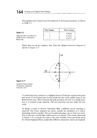
When these are all put together, they form the highpass pole-zero diagram as
shown in Figure 5.17.
Figure 5.17
Seventh-Order Inverse
Chebyshev Highpass
Pole-Zero Plot
In converting from a lowpass to a highpass Inverse Chebyshev response the poles
and zeroes in the S-plane have moved inside the unit circle (unlike those in the
Butterworth case). This is because the pole positions are now in a similar posi-
tion to a lowpass Cauer response. The zero positions are now inside the unit
circle.
To design a Cauer or Inverse Chebyshev filter, a different circuit topology is
required. The Cauer response has zeroes outside the passband, so a notch-
generating circuit is needed. This can be achieved using a circuit that is an exten-
sion of the state variable filter and is known as a biquad. This circuit, illustrated
in Figure 5.18, is exactly the same as the state variable circuit previously given
for all-pole highpass filters, except that different component values are required.