Page 169 - Analog and Digital Filter Design
P. 169
1 66 Analog and Digital Filter Design


                        The gain at DC is denoted by the symbol "A." The resistors labeled R and R'
                        can be any arbitrary value; a typical value may be in the range 1 kR to 100kQ
                        say 10  kR. The resistors labeled R have an effect on the input impedance of the
                        filter section.


                  Denormalizing State Variable or Biquad Designs

                        The simplest approach with state variable and biquad filters is to scale the poles
                        (and zeroes, in the biquad  case) before using the design equations. Choose a
                        capacitor value, and then  use the equations to find the resistor  values. If  the
                        resistor values are very small or very large, select a new capacitor value and try
                        again. Again, aim to keep the resistor values between 1 kR and 100kR.

                        Here's an example of  denormalizing a biquad highpass filter design. Design a
                        second-order Inverse Chebyshev filter that  gives 40 dB stopband  attenuation.
                        This uses normalized lowpass pole locations 0.70705  f j0.71416 and a zero loca-
                        tion  10.04963. The passband cutoff  frequency is  l kHz. Let R = 10 kR and let
                        the reactance of  C = 10 kR at 1 kHz (C = 1/[27rFc. 10'1). Thus, using the nearest
                        E6 preferred value, C = 150 nF.


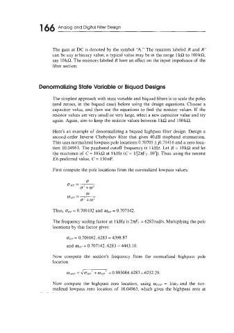
                        First compute the pole locations from the normalized lowpass values:


                        Thus, oIlP = 0.700102 and wHP = 0.707142.

                        The frequency scaling factor at 1 kHz is 2nFc = 6283 radls. Multiplying the pole
                        locations by this factor gives:

                              O/ip = 0.700102.6283 = 4398.87
                              and wHp = 0.707142.6283 = 4443.10.

                        Now  compute  the  section's  frequency  from  the  normalized  highpass  pole
                        location

                              W,,HP = 1/dHp'  + 61,lp'   = 0.995084.6283 = 6252.29.
                        Now  compute  the  highpass  zero  location,  using  oZHp =  l/oz and  the  nor-
                        malized  lowpass zero  location  of  10.04963, which gives the  highpass  zero at

