
Page 173 - Analog and Digital Filter Design
P. 173
1 70 Analog and Digital Filter Design
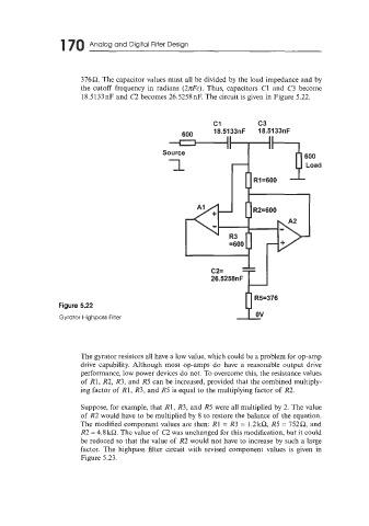
376Q. The capacitor values must all be divided by the load impedance and by
the cutoff frequency in radians (2nFc). Thus, capacitors C1 and C3 become
18.5 133 nF and C2 becomes 26.5258 nF. The circuit is given in Figure 5.22.
1 Load
m
F l
R2=600
!E=376
Figure 5.22
Gyrator Highpass Filter
The gyrator resistors all have a low value, which could be a problem for op-amp
drive capability. Although most op-amps do have a reasonable output drive
performance, low power devices do not. To overcome this, the resistance values
of R1, R2, R3, and R5 can be increased, provided that the combined multiply-
ing factor of R1, R3, and R5 is equal to the multiplying factor of R2.
Suppose, for example, that R1, R3, and R5 were all multiplied by 2. The value
of R2 would have to be multiplied by 8 to restore the balance of the equation.
The modified component values are then: R1 = R3 = 1.2kQ R5 = 752Q and
R2 = 4.8 kQ. The value of C2 was unchanged for this modification, but it could
be reduced so that the value of R2 would not have to increase by such a large
factor. The highpass filter circuit with revised component values is given in
Figure 5.23.