
Page 352 - Analog and Digital Filter Design
P. 352
Filter Integrated Circuits
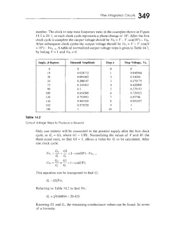
number, The clock to sine wave frequency ratio in the examples shown in Figure
14.5 is 20: 1, so each clock cycle represents a phase change of 18". After the first
clock cycle is complete the output voltage should be Vo, = T.'- V. cos( 18") - P&,.
After subsequent clock cycles the output voltage should be b,? V - Jr. cos(N
=
x IS") - Vo,,,-,,. A table of normalized output voltage steps is given in Table 14.2,
by letting V= I and Voo = 0
Angle, Q degrees Sinusoid Amplitude Step n Step Voltage, Kos
0 0 0 0
18 0.024772 1 0.048944
36 0.095492 2 0.14204
54 0.206107 3 0.270175
72 0.315492 4 0.420808
90 0.5 5 0.579 192
108 0.654508 6 0.729815
126 0.793893 7 0.85796
114 0.904508 8 0.951057
162 0.975528 9 1
180 1 10 1
Table 14.2
Output Voltage Steps to Produce a Sinusoid
Only one resistor will be connected to the positive supply after the first clock
cycle, so G,, = G1, where G1 = UR1. Normalizing the values of V and R1 (let
them equal one), so that G1 = 1, allows a value for G, to be calculated. After
one clock cycle:
This equation can be transposed to find G,:
G, = GI/Vo,
Referring to Table 14.2 to find Pb,:
G, = 1/0.04894 = 20.433.
Knowing G1 and G,. the remaining conductance values can be found. In terms
of a formula: