
Page 60 - Analog and Digital Filter Design
P. 60
Time and Frequency Response 57
circuits. Zero source impedance filter designs are needed to obtain the correct
diplexer response.
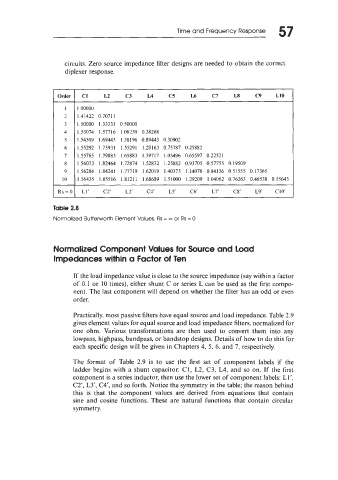
Order c1 L2 C3 L4 C5 L6 C7 L8 C9 L10
1 1 .oooo
- 1.41422 0.7071 1
7
3 1.50000 1.33333 0.50000
4 1.53074 1.57716 1.08339 0.38268
5 1.54509 1.69443 1.38196 0.89443 0.30902
6 1.55292 1.75931 1.55291 1.20163 0.75787 0.25882
7 1.55765 1.79883 1.65883 1.39717 1.05496 0.65597 0.22521
8 1.56073 1.82464 1.72874 1.52832 1.25882 0.93705 0.57755 0.19509
9 1.56284 1.84241 1.77719 1.62019 1.40373 1.14076 0.84136 0.51555 0.17365
10 1.56435 1.85516 1.81211 1.68689 1.51000 1.29209 1.04062 0.76263 0.46538 0.15643
Rs = 0 L1’ C2’ L3’ CY L5’ C6’ L7‘ C8’ L9’ C10’
Table 2.8
Normalized Butterworth Element Values, Rs = - or Rs = 0
Normalized Component Values for Source and Load
Impedances within a Factor of Ten
If the load impedance value is close to the source impedance (say within a factor
of 0.1 or 10 times), either shunt C or series L can be used as the first compo-
nent. The last component will depend on whether the filter has an odd or even
order.
Practically, most passive filters have equal source and load impedance. Table 2.9
gives element values for equal source and load impedance filters, normalized for
one ohm. Various transformations are then used to convert them into any
lowpass, highpass, bandpass, or bandstop designs. Details of how to do this for
each specific design will be given in Chapters 4, 5. 6, and 7, respectively.
The format of Table 2.9 is to use the first set of component labels if the
ladder begins with a shunt capacitor: C1, L2, C3, LA, and so on. If the first
component is a series inductor, then use the lower set of component labels: LI’,
C2’, L3’, C4‘, and so forth. Notice the symmetry in the table; the reason behind
this is that the component values are derived from equations that contain
sine and cosine functions. These are natural functions that contain circular
symmetry.