
Page 69 - Analog and Digital Filter Design
P. 69
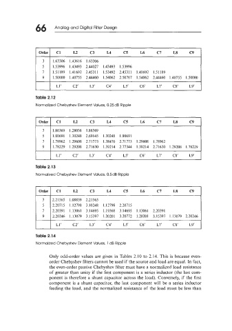
66      Analog and Digital Filter Design


                 I  Order I  C1   L2     c3     L4     C5      16     c7     18     c9  I
                    3   1.63306  1.43616  1.63306
                    5   1.53996  1.43493  2.44027  1.43493  1.53996
                    7   1.51189  1.41692  2.45311  1.53492  2.45311  1.41692  1.51189
                    9   1.50000  1.40755  2.44460  1.54062  2.50767  1.54062  2.44460  1.40755  1.50000
                          LI'    C2'     L3'    C4'    L5'    C6'     L7'    c8'    L9'

                 Table 2.12
                 Normalized Chebyshev Element Values, 0.25 dB Ripple


                 I  Order I  C1   L2     c3     L4     C5      16     c7     18     c9
                    3   1.86369  1.28036  1.86369
                    5   1.80691  1.30248  2.69145  1.30248  1.80691
                    7   1.78962  1.29608  2.71773  1.38476  2.71773  1.29608  1.78962
                    9   1.78229  1.29208  2.71630  1.39214  2.77344  1.39214  2.71630  1.29208  1.78229
                          L1'    C2'    L3'     C4'    L5'    C6'     L7'    C8'    19'
                                                 ~~
                 Table 2.13
                 Normalized Chebyshev Element Values,  0.5 dB Ripple


                  Order   Cl     L2      c3     L4     C5      16     c7     18     c9
                    3   2.21565  1.08839  2.21565
                    5   2.20715  1.12798  3.10248  1.12798  2.20715
                    7   2.20391  1.13061  3.14695  1.19368  3.14695  1.13061  2.20391
                    9   2.20246  1.13079  3.15397  1.20201  3.20772  1.20201  3.15397  1.13079  2.20246
                 I  1            C2'     L3'    C4'    L5'    C6'     L7'    C8'    LY
                          Ll'

                 Table 2.14
                 Normalized Chebyshev Element Values,  1 dB  Ripple

                       Only odd-order  values are given in Tables 2.10 to 2.14. This is because even-
                       order Chebyshev filters cannot be used if the source and load are equal. In fact,
                       the even-order passive Chebyshev filter must have a normalized load resistance
                       of  greater than unity  if the first component is a series inductor (the last com-
                       ponent  is therefore a shunt capacitor across the load). Conversely, if  the first
                       component  is  a shunt capacitor,  the last component  will  be a  series inductor
                       feeding the load, and the normalized  resistance of  the load must be less than