
Page 76 - Analog and Digital Filter Design
P. 76
Time and Frequency Response 73
The component values given in Huelsman and in Tables 2.22 and 2.23 can be
modified to give a filter with a 3dB passband cutoff frequency at 1 rads. This
is possible by using the normalization frequency correction formula, given in
the Appendix. The frequency correction values for some filters are given in Table
2.24. Series inductors and shunt capacitors are reduced in value by multiplying
them by the factor Q~~. To produce useful design tables, I have carried out this
frequency correction; the results are presented later in Tables 2.25 to 2.29.
Consider a fifth-order lowpass filter with a stopband attenuation of 40dB. The
3dB attenuation point occurs at a frequency of 0.61882rad/s and there are two
zeroes beyond the stopband: at 1.05 146 rads and 1.701 3 rads. Normalizing
the design to give a 3dB point at 1 rads by scaling the component values, the
stopband becomes U0.61882, which is about 1.616rads. The zeroes are then
scaled in a similar way to become 1.05146/0.61882 and 1.7013/0.61882, which
are 1.699 rads and 2.749 rads, respectively.
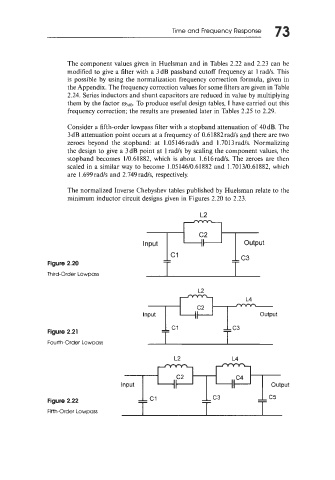
The normalized Inverse Chebyshev tables published by Huelsman relate to the
minimum inductor circuit designs given in Figures 2.20 to 2.23.
Input output
Figure 2.20 T
Third-Order LowDass I I
Input Ifif- output
Figure 2.21 T
Fourth-Order Lowpass T c3
L2 L4
c2 c4
Input II II output
Figure 2.22
Fifth-Order Lowpass