
Page 46 - Applied Photovoltaics
P. 46
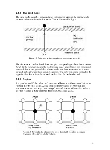
2.1.2  The band model
                          The band model describes semiconductor behaviour in terms of the energy levels
                          between valence and conduction bands. This is illustrated in Fig. 2.2.


                                       Figure 2.2. Schematic of the energy bands for electrons in a solid.


                          The electrons in covalent bonds have energies corresponding to those in the valence
                          band.  In the conduction band the electrons are free. The forbidden gap corresponds
                          to the minimum energy needed to release an electron from a covalent bond to the
                          conducting band where it can conduct a current. The holes remaining conduct in the
                          opposite direction in the valence band, as described for the bond model.
                          2.1.3 Doping

                          It is possible to shift the balance of electrons and holes in a silicon crystal lattice by
                          ‘doping’ it with other atoms. Atoms with one more valence electron than the
                          semiconductor are used to produce ‘n-type’ material. Atoms with one less valence
                          electron result in ‘p-type’ material. This is illustrated in Fig. 2.3.


                                 Figure 2.3. Schematic of a silicon crystal lattice doped with impurities to produce
                                 n-type and p-type semiconductor material.


                                                                                                 33