
Page 49 - Applied Photovoltaics
P. 49
although at present their efficiencies and lifetimes are lower than for crystalline
products. Research into thin film and other potentially low cost solar cell materials
may see these technologies dominate the solar cell market over coming decades.
2.2.4 Thin film crystalline silicon
A very wide range of methods are being investigated to develop thin film silicon cells
deposited on foreign substrates (Green, 2003). If the ratio of hydrogen to silane in the
gas from which amorphous silicon is deposited is increased, the resulting material
becomes microcrystalline, with columns of crystallites separated by amorphous
regions. The optical and electronic properties are similar to those of bulk silicon.
Such material has been used as an alternative to silicon-germanium alloys in hybrid
structures with amorphous silicon. Particular measures are necessary to allow the
amorphous layers to be kept thin enough to avoid light-induced degradation while
producing similar current to the microcrystalline cell(s) in series. A microcrystalline/
amorphous tandem design has been developed with an efficiency of about 11% on a
laboratory scale.
One company is approaching commercial production with a process in which a thin
film silicon cell is formed on a textured glass superstrate. A laser is used to form
craters through the active material to contact the n-type layer closest to the glass. Low
quality material is deposited, then improved by subsequent thermal steps.
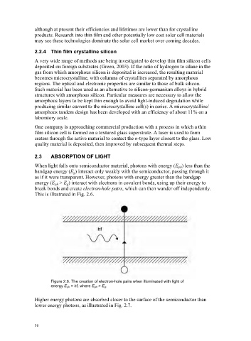
2.3 ABSORPTION OF LIGHT
When light falls onto semiconductor material, photons with energy (E ph ) less than the
bandgap energy (E g ) interact only weakly with the semiconductor, passing through it
as if it were transparent. However, photons with energy greater than the bandgap
energy (E ph > E g ) interact with electrons in covalent bonds, using up their energy to
break bonds and create electron-hole pairs, which can then wander off independently.
This is illustrated in Fig. 2.6.
Figure 2.6. The creation of electron-hole pairs when illuminated with light of
energy E ph = hf, where E ph > E g.
Higher energy photons are absorbed closer to the surface of the semiconductor than
lower energy photons, as illustrated in Fig. 2.7.
36