
Page 51 - Applied Photovoltaics
P. 51
Any defects or impurities within or at the surface of the semiconductor promote
recombination.
The carrier lifetime of a material is defined as the average time for recombination to
occur after electron-hole generation. For silicon, this is typically 1 ȝs. Similarly, the
carrier diffusion length is the average distance a carrier can move from point of
generation until it recombines. For silicon, this is typically 100–300 ȝm. These two
parameters give an indication of material quality and suitability for solar cell use.
However, no power can be produced from a semiconductor without a means of giving
directionality to the moving electrons. Therefore, functional solar cells are typically
produced from semiconductor material by the addition of a rectifying p-n junction.
2.5 P-N JUNCTIONS
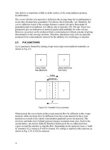
A p-n junction is formed by joining n-type and p-type semiconductor materials, as
shown in Fig. 2.9.
p n
many holes, many electrons,
few electrons few holes
holes
electrons
– +
– +
– +
p – + n
– +
– +
– +
Ê
Figure 2.9. Formation of a p-n junction.
When joined, the excess holes in the p-type material flow by diffusion to the n-type
material, while electrons flow by diffusion from the n-type material to the p-type
material as a result of the carrier concentration gradients across the junction. The
electrons and holes leave behind exposed charges on dopant atom sites, fixed in the
crystal lattice. An electric field (Ê) therefore builds up in the so-called depletion
region around the junction to stop the flow. Depending on the materials used, a ‘built-
in’ potential (V bi ) owing to Ê will be formed. If a voltage is applied to the junction, as
shown in Fig. 2.10, Ê will be reduced.
38