
Page 48 - Applied Photovoltaics
P. 48
boundaries reduce the cell performance by blocking carrier flows, allowing extra
energy levels in the forbidden gap, thereby providing effective recombination sites,
and providing shunting paths for current flow across the p-n junction.
To avoid significant recombination losses at grain boundaries, grain sizes in the order
of a few millimetres are required (Card & Yang, 1977). This also allows single grains
to extend from the front to the back of a cell, providing less resistance to carrier flow
and generally decreasing the length of grain boundaries per unit of cell. Such
multicrystalline material is widely used for commercial solar cell production.
2.2.3 Amorphous silicon
Amorphous silicon can be produced, in principle, even more cheaply than poly-
silicon. With amorphous silicon, there is no long-range order in the structural
arrangement of the atoms, resulting in areas within the material containing
unsatisfied, or ‘dangling’ bonds. These in turn result in extra energy levels within the
forbidden gap, making it impossible to dope the semiconductor when pure, or to
obtain reasonable current flows in a solar cell configuration.
It has been found that the incorporation of atomic hydrogen in amorphous silicon, to a
level of 5–10%, saturates the dangling bonds and improves the quality of the material.
It also increases the bandgap (E g ) from 1.1 eV in crystalline silicon to 1.7 eV, making
the material much more strongly absorbing for photons of energy above the latter
threshold. The thickness of material required to form a functioning solar cell is
therefore much smaller.
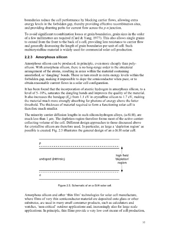
The minority carrier diffusion lengths in such silicon-hydrogen alloys, (a-Si:H), are
much less than 1 ȝm. The depletion region therefore forms most of the active carrier-
collecting volume of the cell. Different design approaches to those discussed above
for crystalline silicon are therefore used. In particular, as large a ‘depletion region’ as
possible is created. Fig. 2.5 illustrates the general design of an a-Si:H solar cell.
p
high field
undoped (intrinsic) ‘depletion’
region
n
Figure 2.5. Schematic of an a-Si:H solar cell.
Amorphous silicon and other ‘thin film’ technologies for solar cell manufacture,
where films of very thin semiconductor material are deposited onto glass or other
substrates, are used in many small consumer products, such as calculators and
watches, ‘non-critical’ outdoor applications and, increasingly also for large scale
applications. In principle, thin films provide a very low cost means of cell production,
35