Page 77 - Applied Photovoltaics
P. 77

l ȡ  w
                                                   R         ȡ                     (4.5)
                                                    b        b
                                                        A     A
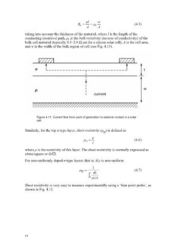
                     taking into account the thickness of the material, where l is the length of the
                     conducting (resistive) path, ȡ b  is the bulk resistivity (inverse of conductivity) of the
                     bulk cell material (typically 0.5–5.0 ȍ.cm for a silicon solar cell), A is the cell area,
                     and w is the width of the bulk region of cell (see Fig. 4.13).


                            Figure 4.11. Current flow from point of generation to external contact in a solar
                            cell.

                     Similarly, for the top n-type layer, sheet resistivity (ȡ ) is defined as
                                                                 †
                                                           ȡ
                                                      ȡ                            (4.6)
                                                       †
                                                           t
                     where ȡ is the resistivity of this layer. The sheet resistivity is normally expressed as
                     ohms/square or ȍ/†.
                     For non-uniformly doped n-type layers; that is, if ȡ is non-uniform

                                                           1
                                                    ȡ                              (4.7)
                                                     †    t dx
                                                         ³ 0  ȡ( x)

                     Sheet resistivity is very easy to measure experimentally using a ‘four point probe’, as
                     shown in Fig. 4.12.


                     64
   72   73   74   75   76   77   78   79   80   81   82