
Page 80 - Applied Photovoltaics
P. 80
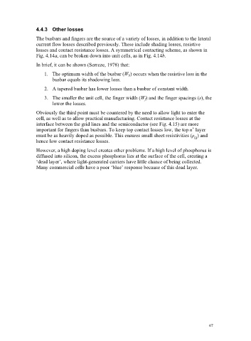
4.4.3 Other losses
The busbars and fingers are the source of a variety of losses, in addition to the lateral
current flow losses described previously. These include shading losses, resistive
losses and contact resistance losses. A symmetrical contacting scheme, as shown in
Fig. 4.14a, can be broken down into unit cells, as in Fig. 4.14b.
In brief, it can be shown (Serreze, 1978) that:
1. The optimum width of the busbar (W b ) occurs when the resistive loss in the
busbar equals its shadowing loss.
2. A tapered busbar has lower losses than a busbar of constant width.
3. The smaller the unit cell, the finger width (W f ) and the finger spacings (s), the
lower the losses.
Obviously the third point must be countered by the need to allow light to enter the
cell, as well as to allow practical manufacturing. Contact resistance losses at the
interface between the grid lines and the semiconductor (see Fig. 4.15) are more
+
important for fingers than busbars. To keep top contact losses low, the top n layer
must be as heavily doped as possible. This ensures small sheet resistivities (ȡ ) and
hence low contact resistance losses.
However, a high doping level creates other problems. If a high level of phosphorus is
diffused into silicon, the excess phosphorus lies at the surface of the cell, creating a
‘dead layer’, where light-generated carriers have little chance of being collected.
Many commercial cells have a poor ‘blue’ response because of this dead layer.
67