
Page 82 - Applied Photovoltaics
P. 82
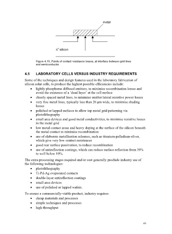
metal


                                              +
                                             n  silicon


                                 Figure 4.15. Points of contact resistance losses, at interface between grid lines
                                 and semiconductor.

                          4.5    LABORATORY CELLS VERSUS INDUSTRY REQUIREMENTS
                          Some of the techniques and design features used in the laboratory fabrication of
                          silicon solar cells, to produce the highest possible efficiencies include:
                              x  lightly phosphorus diffused emitters, to minimise recombination losses and
                                 avoid the existence of a ‘dead layer’ at the cell surface
                              x  closely spaced metal lines, to minimise emitter lateral resistive power losses
                              x  very fine metal lines, typically less than 20 ȝm wide, to minimise shading
                                 losses
                              x  polished or lapped surfaces to allow top metal grid patterning via
                                 photolithography
                              x  small area devices and good metal conductivities, to minimise resistive losses
                                 in the metal grid
                              x  low metal contact areas and heavy doping at the surface of the silicon beneath
                                 the metal contact to minimise recombination
                              x  use of elaborate metallisation schemes, such as titanium-palladium-silver,
                                 which give very low contact resistances
                              x  good rear surface passivation, to reduce recombination
                              x  use of antireflection coatings, which can reduce surface reflection from 30%
                                 to well below 10%.
                          The extra processing stages required and/or cost generally preclude industry use of
                          the following technologies:
                              x  photolithography
                              x  Ti-Pd-Ag evaporated contacts
                              x  double-layer antireflection coatings
                              x  small area devices
                              x  use of polished or lapped wafers.
                          To ensure a commercially-viable product, industry requires:
                              x  cheap materials and processes
                              x  simple techniques and processes
                              x  high throughput


                                                                                                 69