
Page 113 - Build Your Own Transistor Radios a Hobbyists Guide to High-Performance and Low-Powered Radio Circuits
P. 113
• Ll antenna coil: 470 IJH
• Vel two-gang variable capacitor: 140 pF, 60 pF
• Dl, D2: 1N914
• Ql, Q2, Q3: MPSH10
• Q4: MPSH 10 or 2N3904
• VR1: 5 k
1. L 1 Secondary
~/
Feedback VRlIQ3 ~
RF Antenna Filter '\
/ RF Amplifier QlIQ2
L1 -VC1 Audio Out
PowerDet Q4
/
"
+3 Gal n Control VR1
Tap2
C3 1 ut Audio Out
L Secondary m • C3
I
1
10 to 20 Turns m-1 1 C9
+
~ R31K
End2 I C6 1 uf
End1
CB
Ll Primary m VC1A VC1B
•
470 uh R9
Tap1 60 pt lOOK
m ut
C7
+3 .01 uf
03 R5
C12 R7
R1 MPSH10 lOOK
1K
C5
01 R1 4 l01ut
R12
lN914 1K
10K I tOOK
02 Cll
lN914 .01 u;+
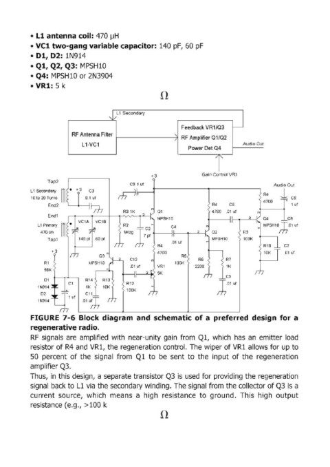
FIGURE 7-6 Block diagram and schematic of a preferred design for a
regenerative radio.
RF signals are amplified with near-unity gain from Q1, which has an emitter load
resistor of R4 and VR1, the regeneration control. The wiper of VR1 allows for up to
50 percent of the signal from Q1 to be sent to the input of the regeneration
amplifier Q3.
Thus, in this design, a separate transistor Q3 is used for providing the regeneration
signa!1 back to Ll via the secondary winding. The signal from the collector of Q3 is a
current source, which means a high resistance to ground. This high output
resistance (e.g., >100 k