Page 153 - Build Your Own Transistor Radios a Hobbyists Guide to High-Performance and Low-Powered Radio Circuits
P. 153

+9


                                                                                            R5
                                                                                           510K
                                                                                         L2
                                  20 pf                                                                VR1
                        60 pt
                                                                                         4 .7 mH        50K
                                                                                 lN270
                                                                                   ca
                                                                                            C9
                                                                                .00331 .00331


                                                                                                 C10
                                                                                                  +
                 Cl                                                        Rl                     1 uf
                   U'
             l01              421F100 Pin Out        +9                   22K
                        To T2  6          3                 R4
                                                            22K
                                          2   ToC2                            01
                                                                             1N914
                        ToOl  4               VC10sc                          02
                                                                             lN914
                                Bottom View
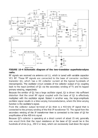
            FIGURE  10-4 Schematic diagram  of the two-transistor supe.rheterodyne

            radio.
            RF  signals  are  received  via  antenna  coil  Ll, which  is  tuned  with  variable  capacitor
            VCl  RF.  These  RF  signals  are  connected  to  the  base  of converter  oscillator
            transistor  Q 1,  which  has  a  DC  collector  current  at  the  typical  hundreds  of

            microamperes.  The  oscillator circuit consists  of the collector output of Ql coupling
            back to the  input (emitter)  of Ql via  the  secondary  winding  of Tl and  its  tapped
            primary winding,  respectively.
            Because  the  emitter of Ql has  a large oscillator signal,  Ql is  driven  into  sufficient
            distortion  that  the  small  RF  signal  coupled  with  the  base  of Ql  is  effectively
            multiplied  with  the  oscillator  signal.  Stated  in  another  way,  the  large-amplitude

            oscillator signal  results  in a time-varying  transconductance,  where the time-varying
            function is the oscillator's signal.
            From  the  collector  output  terminal  of Ql  then  is  a  455-kHz  IF  signal  that  is
            connected to the primary winding of the first IF transformer T2. The signal from the
            secondary  winding  of the  IF transformer then  is  connected  to  the  base  of Q2  for

            amplification of the 455-kHz signal.
            Because  Q2's  collector  is  operating  at  a direct  current  of about  15  mA,  generally
            one  would  think  that  the  input  resistance  at  the  base  of Q2  would  be  in  the
            hundreds of ohms (e.g.,  250 V or less),  which  can  excessively  load  down the signal
   148   149   150   151   152   153   154   155   156   157   158