
Page 138 - Building A Succesful Board-Test Strategy
P. 138
124 BUILDING A SUCCESSFUL BOARD-TEST STRATEGY
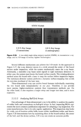
Figure 3-26 A two-sided single inline memory module (SIMM), its transmission x-ray
image, and its 3-D image. (Courtesy Agilent Technologies.)
Several different mechanisms can achieve the 3-D result. In the approach in
Figure 3-27, the x-ray detector moves in a circle around the center of the board
section under inspection, while the system mechanically steers the x-ray beam.
Alternately, a steerable x-ray beam sends signals to eight stationary detectors. In
either case, the system must locate the board surface exactly. The rotating-detector
method scans the board with a laser to map the surface before inspection begins.
The stationary-detector system performs a dynamic surface-mapping that avoids
the test-time overhead of the laser step.
Three-dimensional x-ray can resolve board features individually, examining
the two board sides independently—in one pass. Therefore, it can provide
more precise, higher-resolution analysis than transmission methods can. On
the other hand, it also requires a longer setup and longer test time, and is more
expensive,
3.3.5.3 Analyzing Ball-Grid Arrays
One advantage of three-dimensional x-ray is the ability to analyze the quality
of solder balls and connections on ball-grid arrays. In fact, inspecting BGAs rep-
resents the most common justification argument for adopting x-ray inspection. For
some manufacturers, that is its only regular application. This inspection step looks
for voids, out-of-location solder balls, excess solder, insufficient solder, and shorts.
Figure 3-28 demonstrates how by examining slices at the board surface, the center
of the ball, and the device surface, 3-D x-ray can create an accurate profile.