
Page 244 - Chalcogenide Glasses for Infrared Optics
P. 244
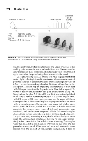
220    Cha pte r  Ni ne


                                                              Evacuated
                                                                quartz
          Cadmium or tellurium                  CdTe samples   chamber


               T 1                            T 2
         T °C    – 700°C CD and Te
         V.P.    – 380 mm CD, 30 mm Te
         Sample
         Thickness – 2, 5, 10, 20 mm


        FIGURE 9.8  Plan to evaluate the effect of Cd and Te vapor on the infrared
        transmission of CdTe produced using AMI three-chamber method.


              must be controlled. Perfect stoichiometry and vapor pressures at the
              melting point must exist at the melt-solid interface. Growth must be
              slow to maintain these conditions. This statement will be emphasized
              again later when the growth of gallium arsenide is discussed.
                 CdTe grown using the AMI process will have Te precipitants that
              scatter light, reducing infrared transmission. Measurements made of
              polished samples of different thickness show an absorption value of
                   −1
              0.3 cm  across the wavelength band of 5 to 8 µm with no free carrier
              absorption. The first step in improving the material is to heat-treat
              with Cd vapor to destroy the Te precipitants. Then follow up with Te
              vapor to restore stoichiometry. The plan is illustrated in Fig. 9.8.
              Samples from the plate 2, 5, 10, and 20 mm thick were cut and polished
              in four sets to be heat-treated for periods of 1, 2, 4, and 8 days at 700°C
              with Cd vapor at 380-mm vapor pressure and Te vapor at 30-mm
              vapor pressure. A fifth set of samples was prepared to be a reference
              with no vapor treatment. The samples were placed in the tubes along
              with a piece of Cd or Te, sealed, and evacuated. After the tests were
              complete, the samples were removed, infrared transmission was
              measured, and results were compared. All the Cd treated samples
              showed free carrier absorption in the 5- to 8-µm band after only
              2  days’ treatment, increasing in magnitude with each day of treat-
              ment. The untreated did not change, showing no free carrier absorp-
              tion just low transmission due to Te inclusion scattering. The samples
              were then reloaded in the chambers only with Te this time, and the
              procedure was repeated. All samples had a marked increase in trans-
              mission with the thickest, 20-mm sample taking nearly 8 days to