Page 139 - Complementarity and Variational Inequalities in Electronics
P. 139

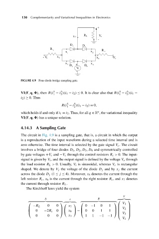
130  Complementarity and Variational Inequalities in Electronics


                           FIGURE 4.9 Four-diode-bridge sampling gate.


                                            5   5                               5   5
                           VI(F,q, ), then R(i − i )(i 1 − i 2 ) ≤ 0. It is clear also that R(i − i )(i 1 −
                                            1   2                               1   2
                           i 2 ) ≥ 0. Thus
                                                        5
                                                    5
                                                 R(i − i )(i 1 − i 2 ) = 0,
                                                    1  2
                                                                    n
                           which holds if and only if i 1 = i 2 . Thus, for all q ∈ R , the variational inequality
                           VI(F,q, ) has a unique solution.
                           4.14.3 A Sampling Gate
                           The circuit in Fig. 4.9 is a sampling gate, that is, a circuit in which the output
                           is a reproduction of the input waveform during a selected time interval and is
                           zero otherwise. The time interval is selected by the gate signal V c . The circuit
                           involves a bridge of four diodes D 1 ,D 2 ,D 3 ,D 4 and symmetrically controlled
                           by gate voltages +V c and −V c through the control resistors R c > 0. The input-
                           signal is given by V i , and the output signal is defined by the voltage V o through
                           the load resistor R L > 0. Usually, V i is sinusoidal, whereas V c is rectangular
                           shaped. We denote by V j the voltage of the diode D j and by x j the current
                           across the diode D j (1 ≤ j ≤ 4). Moreover, x 5 denotes the current through the
                           left resistor R c , x 6 is the current through the right resistor R c , and x 7 denotes
                           the current through resistor R L .
                              The Kirchhoff laws yield the system

                                                                                  V
                                        A            x              B
                                                                               ⎛     ⎞

                                                                                  V 1
                               ⎛                ⎞          ⎛                 ⎞
                                                       ⎞
                                                  ⎛
                                 −R L    0    0     x 7       0  −1   0   1
                                                                               ⎜     ⎟
                                   0   −2R c      ⎝  x 6  ⎠ − ⎝ 0  0  1
                               ⎜                ⎟          ⎜                 ⎟⎜ V 2 ⎟
                               ⎝              0 ⎠                         1 ⎠⎜       ⎟
                                   0     0    0     x 1       1  1   −1   −1   ⎝ V 3 ⎠
                                                                                  V 4
   134   135   136   137   138   139   140   141   142   143   144