
Page 121 - Complete Wireless Design
P. 121
Amplifier Design
120 Chapter Three
Use vector quantities to calculate .
S
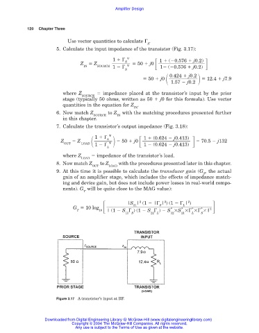
5. Calculate the input impedance of the transistor (Fig. 3.17):
1
1 ( 0.576 j0.2)
S
Z Z 50 j0
IN SOURCE 1
1 ( 0.576 j0.2)
S
0.424 j0.2
50 j0 12.4 j7.9
1.57 j0.2
where Z impedance placed at the transistor’s input by the prior
SOURCE
stage (typically 50 ohms, written as 50 j0 for this formula). Use vector
quantities in the equation for Z .
IN
6. Now match Z to Z with the matching procedures presented further
SOURCE IN
in this chapter.
7. Calculate the transistor’s output impedance (Fig. 3.18):
1
1 (0.624 j0.413)
L
Z Z LOAD 50 j0 70.5 j132
OUT 1
1 (0.624 j0.413)
L
where Z impedance of the transistor’s load.
LOAD
8. Now match Z to Z with the procedures presented later in this chapter.
OUT LOAD
9. At this time it is possible to calculate the transducer gain (G , the actual
T
gain of an amplifier stage, which includes the effects of impedance match-
ing and device gain, but does not include power losses in real-world compo-
nents). G will be quite close to the MAG value):
T
2
2
2
|S | (1 | | ) (1 | )
S
L
21
G 10 log 10
*
*
*
*
T | (1 S ) (1 S ) S S | 2
11 S 22 L 12 21 L S
Figure 3.17 A transistor’s input at RF.
Downloaded from Digital Engineering Library @ McGraw-Hill (www.digitalengineeringlibrary.com)
Copyright © 2004 The McGraw-Hill Companies. All rights reserved.
Any use is subject to the Terms of Use as given at the website.