Page 118 - Complete Wireless Design
P. 118

Amplifier Design


                                                                               Amplifier Design  117

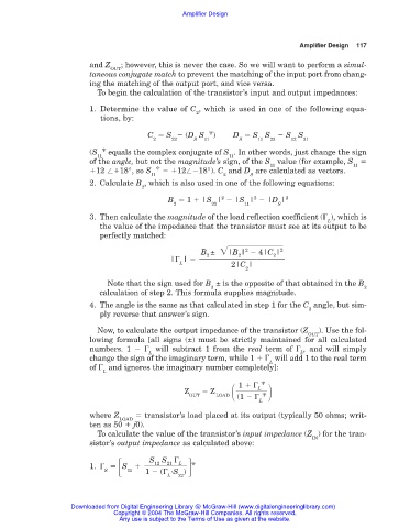
                        and Z   ; however, this is never the case. So we will want to perform a simul-
                              OUT
                        taneous conjugate match to prevent the matching of the input port from chang-
                        ing the matching of the output port, and vice versa.
                          To begin the calculation of the transistor’s input and output impedances:

                        1. Determine the value of C , which is used in one of the following equa-
                                                    2
                           tions, by:
                                       C   S   (D S    
 )    D   S S   S S
                                         2    22   S  11       S    11  22   12  21
                        (S  
  equals the complex conjugate of S . In other words, just change the sign
                          11                                11
                        of the angle, but not the magnitude’s sign, of the S value (for example, S
                                                                                             11
                                                                       11
                         12   18°, so S   
    12  18°). C and D are calculated as vectors.
                                        11                 2      S
                        2. Calculate B , which is also used in one of the following equations:
                                      2
                                                           2
                                                                   2
                                             B   1   |S |   |S |   |D |    2
                                              2         22       11      S
                        3. Then calculate the magnitude of the load reflection coefficient (  ), which is
                                                                                      L
                           the value of the impedance that the transistor must see at its output to be
                           perfectly matched:

                                                     B ±  |B |    4|C |   2
                                                                 2
                                                               2
                                                       2
                                                                        2
                                             |  |
                                                L            2|C |
                                                                 2
                             Note that the sign used for B ± is the opposite of that obtained in the B
                                                        2                                       2
                           calculation of step 2. This formula supplies magnitude.
                        4. The angle is the same as that calculated in step 1 for the C angle, but sim-
                                                                                 2
                           ply reverse that answer’s sign.
                          Now, to calculate the output impedance of the transistor (Z  ). Use the fol-
                                                                                 OUT
                        lowing formula [all signs (±) must be strictly maintained for all calculated
                        numbers. 1     will subtract 1 from the  real term of    , and will simply
                                        L                                      L
                        change the sign of the imaginary term, while 1    will add 1 to the real term
                                                                       L
                        of   and ignores the imaginary number completely]:
                            L

                                                               1
                                                                    L
                                                 Z     Z LOAD
                                                  OUT          (1
                                                                    L
                        where Z       transistor’s load placed at its output (typically 50 ohms; writ-
                                LOAD
                        ten as 50   j0).
                          To calculate the value of the transistor’s input impedance (Z ) for the tran-
                                                                                  IN
                        sistor’s output impedance as calculated above:
                            S           S S     L
                                         12
                                            21
                        1.     S
                                  11
                                       1   (   S )
                                             L  22
                   Downloaded from Digital Engineering Library @ McGraw-Hill (www.digitalengineeringlibrary.com)
                               Copyright © 2004 The McGraw-Hill Companies. All rights reserved.
                                Any use is subject to the Terms of Use as given at the website.
   113   114   115   116   117   118   119   120   121   122   123