
Page 129 - Complete Wireless Design
P. 129
Amplifier Design
128 Chapter Three
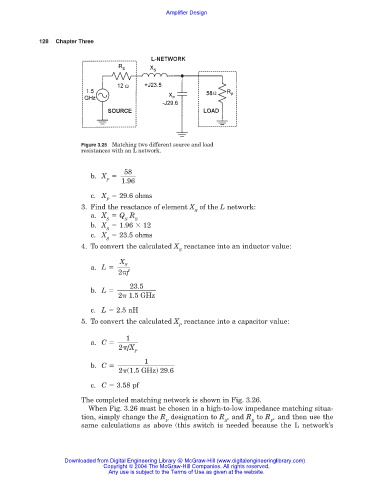
Figure 3.25 Matching two different source and load
resistances with an L network.
58
b. X
P 1.96
c. X 29.6 ohms
P
3. Find the reactance of element X of the L network:
S
a. X Q R
S S S
b. X 1.96 12
S
c. X 23.5 ohms
S
4. To convert the calculated X reactance into an inductor value:
S
X
S
a. L
2 f
23.5
b. L
2 1.5 GHz
c. L 2.5 nH
5. To convert the calculated X reactance into a capacitor value:
P
1
a. C
2 fX
P
1
b. C
2 (1.5 GHz) 29.6
c. C 3.58 pf
The completed matching network is shown in Fig. 3.26.
When Fig. 3.26 must be chosen in a high-to-low impedance matching situa-
tion, simply change the R designation to R , and R to R , and then use the
P S S P
same calculations as above (this switch is needed because the L network’s
Downloaded from Digital Engineering Library @ McGraw-Hill (www.digitalengineeringlibrary.com)
Copyright © 2004 The McGraw-Hill Companies. All rights reserved.
Any use is subject to the Terms of Use as given at the website.