
Page 131 - Complete Wireless Design
P. 131
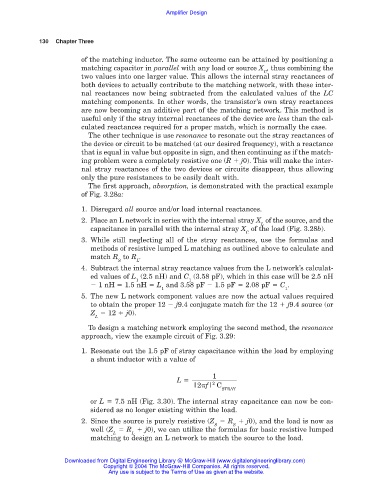
Amplifier Design


            130  Chapter Three

                        of the matching inductor. The same outcome can be attained by positioning a
                        matching capacitor in parallel with any load or source X , thus combining the
                                                                            C
                        two values into one larger value. This allows the internal stray reactances of
                        both devices to actually contribute to the matching network, with these inter-
                        nal reactances now being subtracted from the calculated values of the  LC
                        matching components. In other words, the transistor’s own stray reactances
                        are now becoming an additive part of the matching network. This method is
                        useful only if the stray internal reactances of the device are less than the cal-
                        culated reactances required for a proper match, which is normally the case.
                          The other technique is use resonance to resonate out the stray reactances of
                        the device or circuit to be matched (at our desired frequency), with a reactance
                        that is equal in value but opposite in sign, and then continuing as if the match-
                        ing problem were a completely resistive one (R   j0). This will make the inter-
                        nal stray reactances of the two devices or circuits disappear, thus allowing
                        only the pure resistances to be easily dealt with.
                          The first approach, absorption, is demonstrated with the practical example
                        of Fig. 3.28a:

                        1. Disregard all source and/or load internal reactances.
                        2. Place an L network in series with the internal stray X of the source, and the
                                                                            L
                           capacitance in parallel with the internal stray X of the load (Fig. 3.28b).
                                                                       C
                        3. While still neglecting all of the stray reactances, use the formulas and
                           methods of resistive lumped L matching as outlined above to calculate and
                           match R to R .
                                   S    L
                        4. Subtract the internal stray reactance values from the L network’s calculat-
                           ed values of L (2.5 nH) and C (3.58 pF), which in this case will be 2.5 nH
                                        1              1
                             1 nH   1.5 nH   L and 3.58 pF   1.5 pF   2.08 pF   C .
                                               1                                  1
                        5. The new L network component values are now the actual values required
                           to obtain the proper 12   j9.4 conjugate match for the 12   j9.4 source (or
                           Z   12   j0).
                            L
                          To design a matching network employing the second method, the resonance
                        approach, view the example circuit of Fig. 3.29:

                        1. Resonate out the 1.5 pF of stray capacitance within the load by employing
                           a shunt inductor with a value of
                                                              1
                                                    L
                                                              2
                                                        |2 f| C
                                                                STRAY
                           or L   7.5 nH (Fig. 3.30). The internal stray capacitance can now be con-
                           sidered as no longer existing within the load.
                        2. Since the source is purely resistive (Z   R   j0), and the load is now as
                                                              S     S
                           well (Z   R   j0), we can utilize the formulas for basic resistive lumped
                                 L     L
                           matching to design an L network to match the source to the load.

                   Downloaded from Digital Engineering Library @ McGraw-Hill (www.digitalengineeringlibrary.com)
                               Copyright © 2004 The McGraw-Hill Companies. All rights reserved.
                                Any use is subject to the Terms of Use as given at the website.